Blog

Archive for the ‘materials’ category: Page 119

Nov 11, 2022

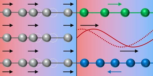
Study demonstrates tailored Ising superconductivity in intercalated bulk niobium diselenide

Posted by in categories: materials, quantum physics

When 2D layered materials are made thinner (i.e., at the atomic scale), their properties can dramatically change, sometimes resulting in the emergence of entirely new features and in the loss of others. While new or emerging properties can be very advantageous for the development of new technologies, retaining some of the material’s original properties is often equally important.

Researchers at Tsinghua University, the Chinese Academy of Sciences and the Frontier Science Center for Quantum Information have recently been able to realize tailored Ising superconductivity in a sample of intercalated bulk niobium diselenide (NbSe2), a characteristic of bulk NbSe2 that is typically compromised in . The methods they used, outlined in a paper published in Nature Physics, could pave the way towards the fabrication of 2D thin-layered superconducting materials.

“Atomically thin 2D materials exhibit interesting properties that are often distinct from their bulk materials, which consist of hundreds and thousands of layers,” Shuyun Zhou, one of the researchers who carried out the study, told Phys.org. “However, atomically thin films/flakes are difficult to fabricate, and the emerging new properties are sometimes achieved by sacrificing some other important properties.”

Nov 11, 2022

Overcoming Scale-Up Challenges in Gene Therapy Manufacturing

Posted by in categories: biotech/medical, materials

My good friend Logan collins posted this.


Gene therapies can scale economically, but not just with practices adapted from traditional biologics. According to Avantor, gene therapies pose unique material, workflow, and partnering challenges.

Nov 10, 2022

Scientists Create Crystals That Generate Electricity From Heat

Posted by in category: materials

In the effort to efficiently convert heat into electricity, easily accessible materials from harmless raw materials open up new perspectives in the development of safe and inexpensive so-called thermoelectric materials. A synthetic copper mineral acquires a complex structure and microstructure through simple changes in its composition, thereby laying the foundation for the desired properties, according to a study published recently in the journal Angewandte Chemie.

The novel synthetic material is composed of copper, manganese, germanium, and sulfur, and it is produced in a rather simple process, explains materials scientist Emmanuel Guilmeau, CNRS researcher at CRISMAT laboratory, Caen, France, who is the corresponding author of the study. The powders are simply mechanically alloyed by ball-milling to form a precrystallized phase, which is then densified by 600 degrees Celsius.

The Celsius scale, also known as the centigrade scale, is a temperature scale named after the Swedish astronomer Anders Celsius. In the Celsius scale, 0 °C is the freezing point of water and 100 °C is the boiling point of water at 1 atm pressure.

Nov 10, 2022

Researchers create device to replicate conditions in blood vessels after grafts

Posted by in categories: biotech/medical, materials

Tohid Didar and Jeff Weitz had a solution, but they also had a problem.

Didar, an associate professor of engineering and Weitz, a hematologist, professor of medicine and executive director of the Thrombosis & Atherosclerosis Research Institute, had collaborated to create a novel and highly promising material to improve the success of vascular grafts, but they needed a better way to test how well it worked.

Their revolutionary idea was an engineered non-stick surface combined with biological components that can repel all but a targeted group of cells — those that form the natural lining of the body’s veins and arteries.

Nov 9, 2022

Atomic changes in metals could lead to longer-lasting batteries

Posted by in categories: materials, transportation

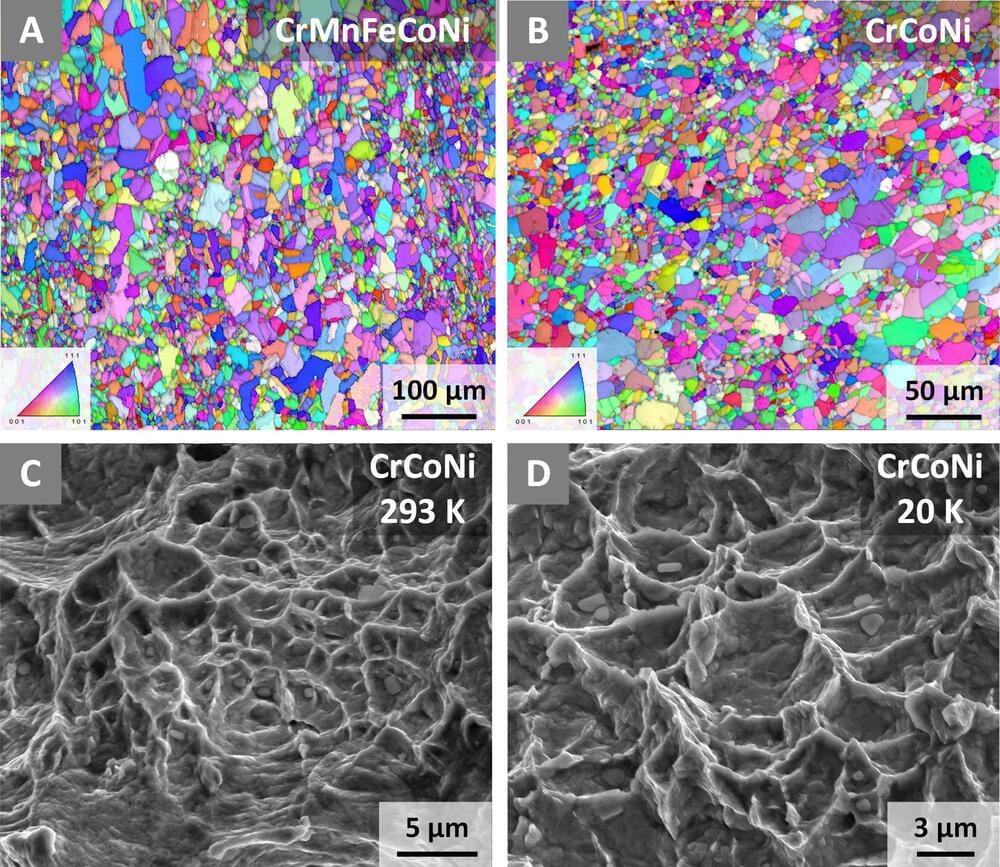
Researchers at Pacific Northwest National Laboratory (PNNL) are studying the atomic-level changes in metals undergoing shear deformation in order to deduce the effects of physical forces on these materials, according to a report by Phys.org published on Monday.

The work could lead to many new and improved applications such as longer-lasting batteries and lighter vehicles.

Nov 9, 2022

Magnetism or no magnetism? The influence of substrates on electronic interactions

Posted by in categories: energy, materials

A new study at Monash University illustrates how substrates affect strong electronic interactions in two-dimensional metal-organic frameworks.

Materials with strong electronic interactions can have applications in energy-efficient electronics. When these materials are placed on a , their are changed by charge transfer, strain, and hybridization.

The study also shows that electric fields and applied strain could be used to “switch” interacting phases such as on and off, allowing potential applications in future energy-efficient electronics.

Nov 9, 2022

Materials Made of Mechanical Neural Networks Can Learn to Adapt Their Physical Properties

Posted by in categories: materials, robotics/AI

A new type of material can learn and improve its ability to deal with unexpected forces thanks to a unique lattice structure with connections of variable stiffness, as described in a new paper by my colleagues and me.

The new material is a type of architected material, which gets its properties mainly from the geometry and specific traits of its design rather than what it is made out of. Take hook-and-loop fabric closures like Velcro, for example. It doesn’t matter whether it is made from cotton, plastic or any other substance. As long as one side is a fabric with stiff hooks and the other side has fluffy loops, the material will have the sticky properties of Velcro.

My colleagues and I based our new material’s architecture on that of an artificial neural network—layers of interconnected nodes that can learn to do tasks by changing how much importance, or weight, they place on each connection. We hypothesized that a mechanical lattice with physical nodes could be trained to take on certain mechanical properties by adjusting each connection’s rigidity.

Nov 7, 2022

Gate-tunable heterojunction tunnel triodes based on 2D metal selenide and 3D silicon

Posted by in categories: computing, materials

Electronics engineers worldwide are trying to improve the performance of devices, while also lowering their power consumption. Tunnel field-effect transistors (TFETs), an experimental class of transistors with a unique switching mechanism, could be a particularly promising solution for developing low-power electronics.

Despite their potential, most TFETs based on silicon and III-V heterojunctions exhibit low on-current densities and on/off current ratios in some modes of operation. Fabricating these transistors using 2D materials could help to improve electrostatic control, potentially increasing their on-current densities and on/off ratios.

Researchers at University of Pennsylvania, the Chinese Academy of Sciences, the National Institute of Standards and Technology, and the Air Force Research Laboratory have recently developed new heterojunction tunnel triodes based on van der Waals heterostructures formed from 2D metal selenide and 3D silicon. These triodes, presented in a paper published in Nature Electronics, could outperform other TFETs presented in the past in terms of on-current densities and on/off ratios.

Nov 7, 2022

Artificial intelligence deciphers detector ‘clouds’ to accelerate materials research

Posted by in categories: materials, robotics/AI

X-rays can be used like a superfast, atomic-resolution camera, and if researchers shoot a pair of X-ray pulses just moments apart, they get atomic-resolution snapshots of a system at two points in time. Comparing these snapshots shows how a material fluctuates within a tiny fraction of a second, which could help scientists design future generations of super-fast computers, communications, and other technologies.

Resolving the information in these X-ray snapshots, however, is difficult and time intensive, so Joshua Turner, a lead scientist at the Department of Energy’s SLAC National Accelerator Center and Stanford University, and ten other researchers turned to artificial intelligence to automate the process. Their machine learning-aided method, published October 17 in Structural Dynamics, accelerates this X-ray probing technique, and extends it to previously inaccessible materials.

“The most exciting thing to me is that we can now access a different range of measurements, which we couldn’t before,” Turner said.

Nov 7, 2022

New camera system taps into terahertz wavelengths for better imaging

Posted by in categories: materials, security

A team of engineers has developed a new type of camera that can detect radiation in terahertz (THz) wavelengths. This new imaging system can see through certain materials in high detail, which could make it useful for security scanners and other sensors.

Terahertz radiation is that which has wavelengths between microwaves and visible light, and these frequencies show promise in a new class of imaging systems. They can penetrate many materials and capture new levels of detail, and importantly the radiation is non-ionizing, meaning it’s safer than X-rays when used on humans.

The problem is that detectors that pick up THz wavelengths can be bulky, slow, expensive, difficult to run under practical conditions, or some combination of these. But in a new study, researchers at MIT, Samsung and the University of Minnesota have developed a system that can detect THz pulses quickly, precisely and at regular room temperature and pressure.