Quantum materials, materials exhibiting physical behavior governed by the laws of quantum mechanics, have proved promising for the development of numerous advanced technologies, including quantum technologies, memory devices and solar panels. In some of these materials, electrons can collectively arrange themselves in unusual patterns, giving rise to states that cannot be explained by classical physics theories.
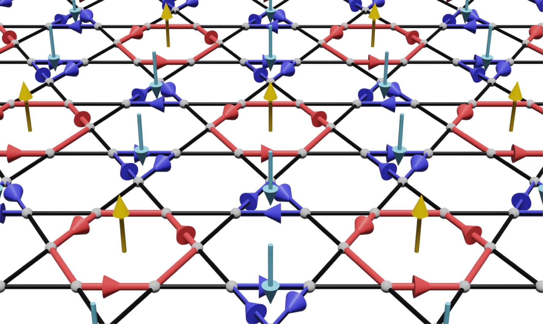
For more than two decades, theoretical physicists have predicted the existence of a loop current order in some quantum materials. This is a state characterized by tiny electrical currents circulating around microscopic loops inside a crystal, which would produce no measurable electric current flowing through a material.
These current loops were predicted to emerge when electrons spontaneously organize themselves into a less symmetrical pattern than the crystal itself, even if atoms remain in similar positions. While this phenomenon was widely studied and described by theorists in the past, it has so far proved difficult to observe experimentally.