Researchers have designed a diamond-based quantum sensor that could help detect altermagnets, a newly discovered type of magnetic material with unusual properties.
Category: materials


Polymer network reconfigures in sequence, helping elastomers stay tough under strain
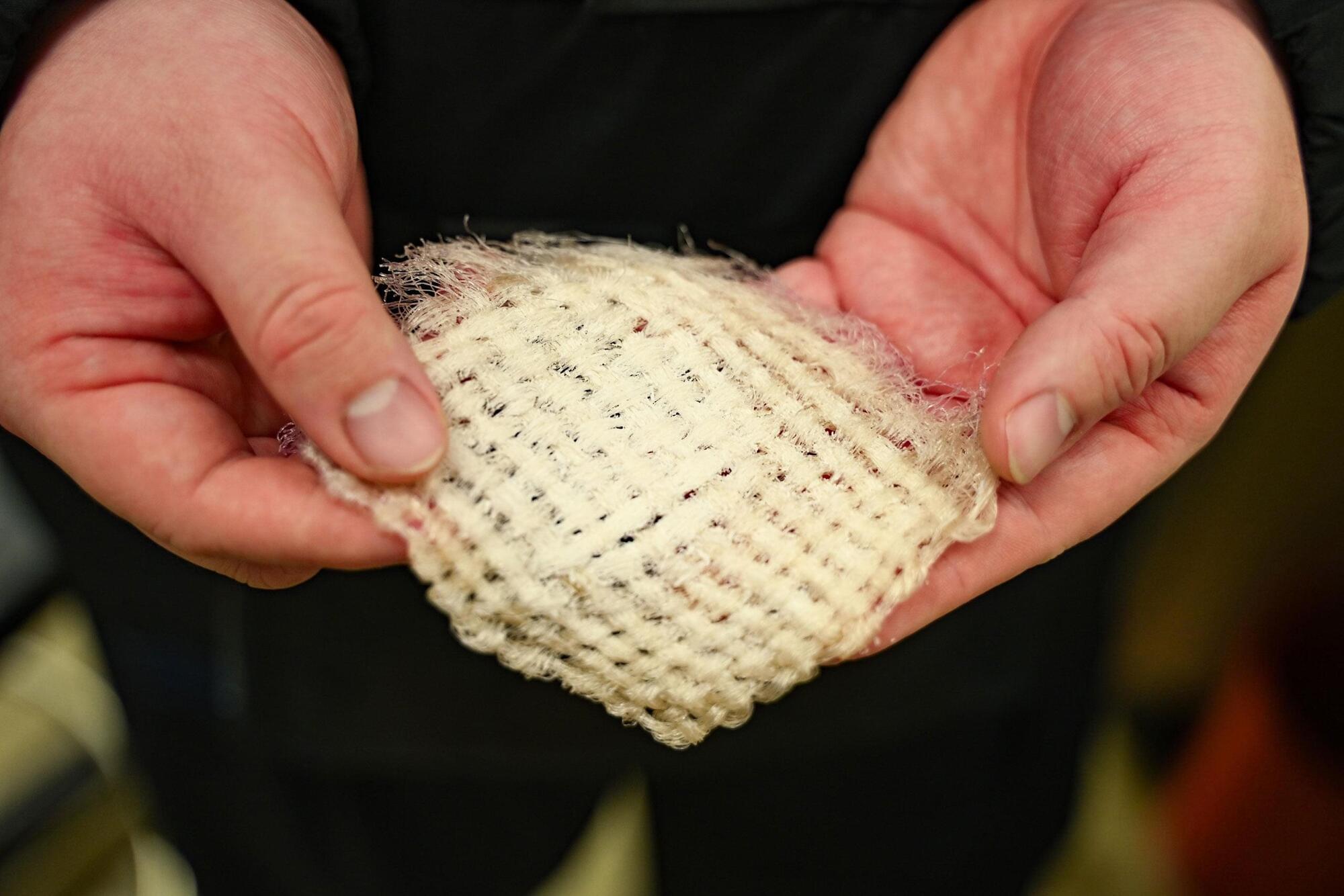
Shock-absorbing sneaker soles are likely made of polyurethane, a highly elastic and tough polymer. The ability of these elastomers to absorb impact without breaking is extremely important for practical applications. While multiple strategies exist for enhancing elastomer toughness, each has its limitations. However, achieving synergistic toughening by integrating all three mechanisms within a single material remains challenging.
Now, researchers at the University of Osaka have overcome these limitations by developing a multipath synergistic strategy to toughen elastomers. This discovery is reported in Nature Communications.
Elastomers are polymers that are exceptionally elastic; they can deform strongly under external stress and revert to their original shape when the stress is removed. However, traditional elastomers are not very tough because microscopic cracks can cause the material to tear.

Microstructure-based model predicts sheet metal behavior in seconds for car and battery design
A research team led by Kyung Mun Min and Seonghwan Choi of Materials Processing Research Division (Korea Institute of Materials Science) has developed a new analysis model capable of predicting the anisotropic mechanical behavior of sheet metals within seconds using only microstructural information of metallic materials.
The technology is expected to reduce the time and cost required to design forming processes for metallic materials used in automobiles and batteries by enabling fast, accurate prediction of how sheet metals stretch and deform without complex, repetitive experiments.
The study is published in the International Journal of Plasticity.
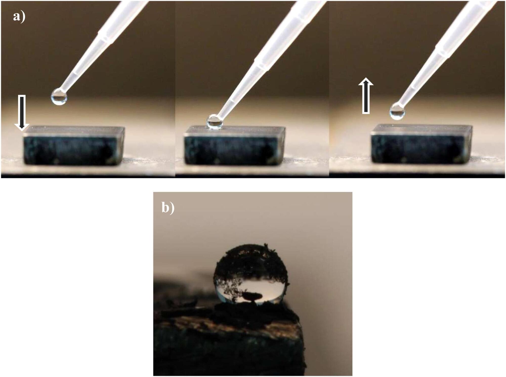
Plasma and graphene combine to protect metal surfaces from corrosion
Plasma is an ionized gas, often referred to as the fourth state of matter. Plasmas, which are created artificially by applying energy to a gas, are found in the fluorescent tubes that illuminate kitchens. However, they have many other possible applications, such as the production of graphene.
The Plasma Innovation Laboratory (LIPs) at the University of Córdoba has already made progress in using plasma to produce graphene, the revolutionary material that earned its discoverers the Nobel Prize. Recently, a new technological design boosted graphene production by more than 22%. Continuing along this line of research, the team is now proposing two methods for applying graphene—also highly anticorrosive—to metal surfaces using microwave plasmas at atmospheric pressure, with the aim of not altering the properties of the metals.
The research is published in the journal Surfaces and Interfaces.

Molecular mechanics behind heart cell restructuring revealed
Microtubules, part of heart muscle cells’ internal “skeleton,” help determine how the heart changes shape under stress, and a common signaling pathway called the ERK pathway acts as a key controller of where the building materials for these cells’ growth are delivered inside them, a pair of new studies show. These findings, from a team at the Perelman School of Medicine at the University of Pennsylvania, point to possible new ways to address harmful heart remodeling that can be linked to heart failure.
“The molecular decision behind how a heart cell, and by extension the heart, changes in size and shape has been a mystery, even though we’ve known that heart cells do change in length and width over a person’s life in response to different conditions,” said the studies’ senior author Benjamin Prosser, Ph.D., a professor of Physiology.
“But now that we know what is doing the work and what guides it, that opens the door to targeting these mechanisms and correcting abnormal growth.”
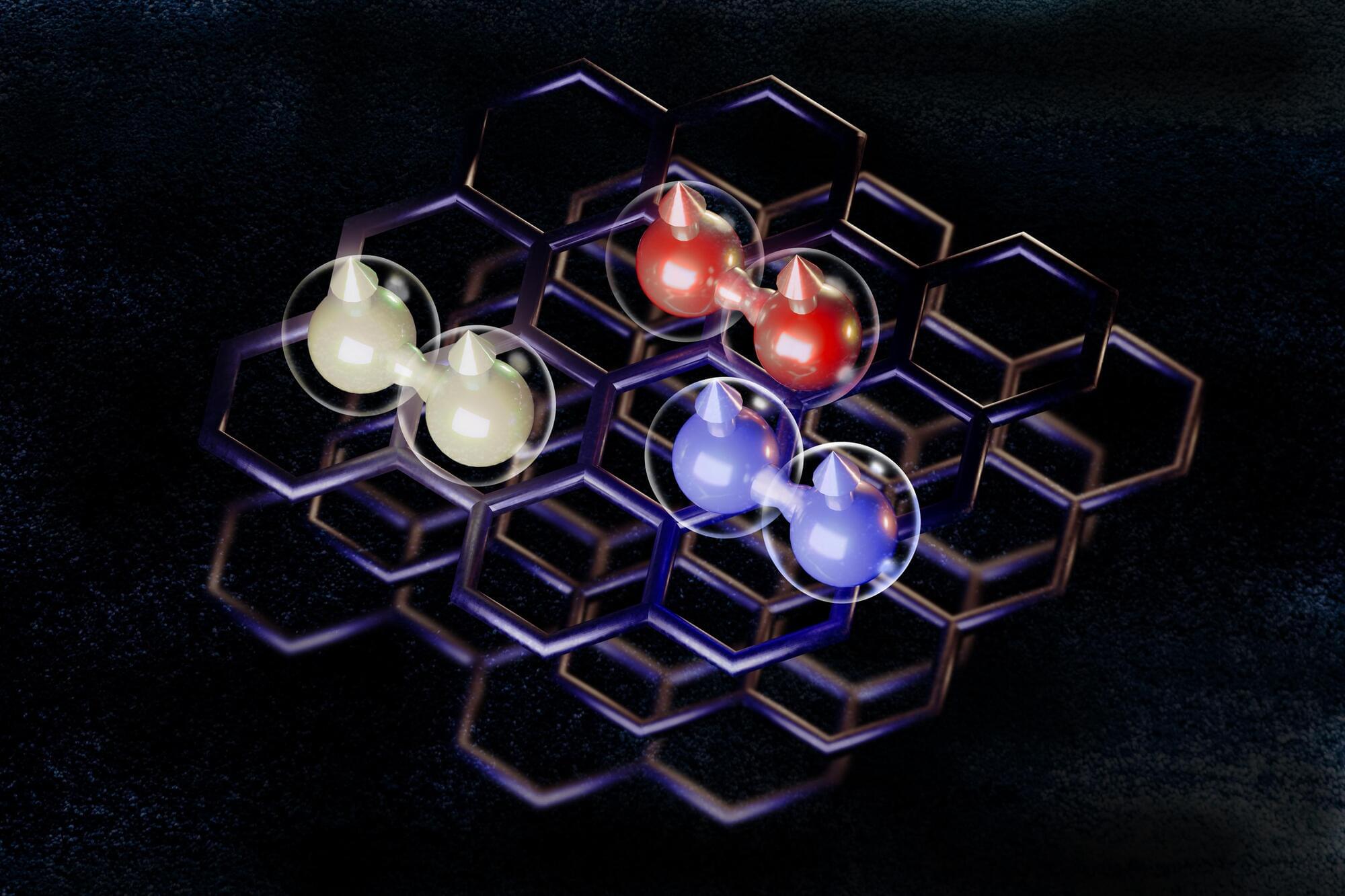
Graphene can hold multiple states of superconductivity, a new study finds
The researchers discovered the multiple superconducting states in atomically thin exfoliations of graphite, known as graphene. Specifically, graphene is a single-atom-thin sheet of carbon atoms arranged precisely in a microscopic lattice. The team made its discoveries in samples of rhombohedral graphene, which is a natural structure within graphite consisting of a stack of four or five graphene layers.
Interestingly, the researchers found that several of the new superconducting states in rhombohedral graphene are able to persist in the presence of a magnetic field, which normally kills superconductivity.
And in a further surprise, these superconducting states even get stronger when exposed to a magnetic field.
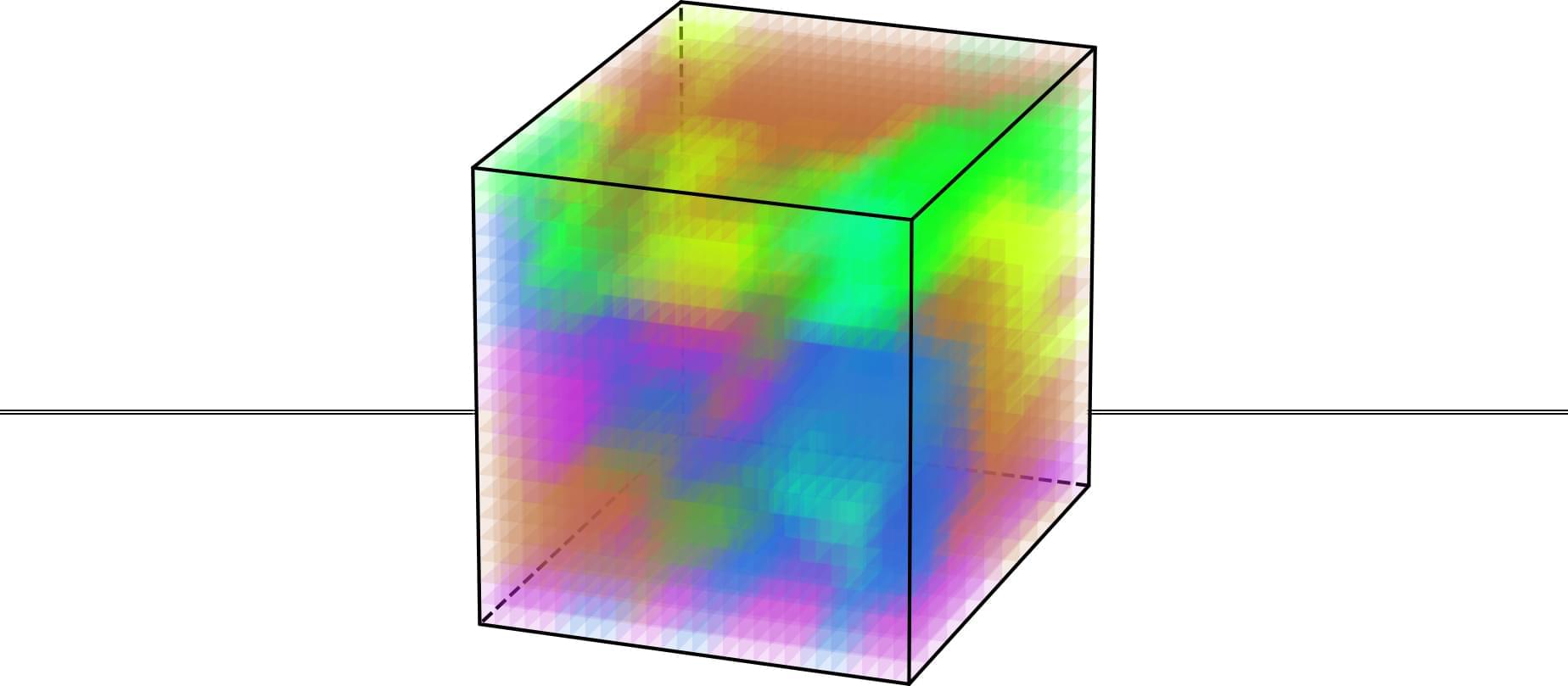
The hidden structure behind a widely used class of materials
Materials called relaxor ferroelectrics have been used for decades in technologies like ultrasounds, microphones, and sonar systems. Their unique properties come from their atomic structure, but that structure has stubbornly eluded direct measurement.
Now a team of researchers from MIT and elsewhere has directly characterized the three-dimensional atomic structure of a relaxor ferroelectric for the first time. The findings, reported today in Science, provide a framework for refining models used to design next-generation computing, energy, and sensing devices.
“Now that we have a better understanding of exactly what’s going on, we can better predict and engineer the properties we want materials to achieve,” says corresponding author James LeBeau, MIT’s Kyocera Professor of Materials Science and Engineering. “The research community is still developing methods to engineer these materials, but in order to predict the properties those materials will have, you have to know if your model is right.”