Toggle light / dark theme

Blood–Brain Barrier-Targeting Nanoparticles: Biomaterial Properties and Biomedical Applications in Translational Neuroscience

This case-control study found that adults with schizophrenia had significantly greater frontal cortex serotonin release than healthy controls, and greater release correlated with more severe negative symptoms.


Question Is serotonin release altered in vivo in schizophrenia, and is it associated with negative symptom severity?

Findings In this case-control neuroimaging study that included 54 adults, frontal cortex serotonin release was significantly greater in the 26 people with DSM-5 schizophrenia compared with 28 matched healthy controls. In schizophrenia, greater frontal cortex serotonin release was associated with more severe baseline negative symptoms.

Meaning Findings suggest that serotonergic dysfunction in the pathophysiology of schizophrenia was associated with negative symptoms, identifying the regulation of serotonergic neurotransmission as a potential target to treat negative symptoms.

From fullerenes to 2D structures: A unified design principle for boron nanostructures

Boron, a chemical element next to carbon in the periodic table, is known for its unique ability to form complex bond networks. Unlike carbon, which typically bonds with two or three neighboring atoms, boron can share electrons among several atoms. This leads to a wide variety of nanostructures. These include boron fullerenes, which are hollow, cage-like molecules, and borophenes, ultra-thin metallic sheets of boron atoms arranged in triangular and hexagonal patterns.

Dr. Nevill Gonzalez Szwacki has developed a model explaining the variety of boron nanostructures. The analysis, published in the journal 2D Materials, combines more than a dozen known boron nanostructures, including the experimentally observed B₄₀ and B₈₀ fullerenes.

Using first-principles quantum-mechanical calculations, the study shows that the structural, energetic, and electronic properties of these systems can be predicted by looking at the proportions of atoms with four, five, or six bonds. The results reveal clear links between finite and extended boron structures. The B₄₀ cage corresponds to the χ₃ borophene layer, while B₆₅, B₈₀, and B₉₂ connect with the β₁₂, α, and bt borophene sheets, respectively. These structural links suggest that new boron cages could be created by using known two-dimensional boron templates.

Real-life ‘quantum molycircuits’ using exotic nanotubes

Molybdenum disulfide MoS2 is a groundbreaking material for electronics applications. As a two-dimensional layer similar to graphene, it is an excellent semiconductor, and can even become intrinsically superconducting under the right conditions. It’s not particularly surprising that science fiction authors have already been speculating about molycircs, fictional computer circuits built from MoS2, for years—and that physicists and engineers are directing huge research efforts at this material.

Researchers at the University of Regensburg, have many years of expertise with diverse quantum materials—in particular also with carbon nanotubes, tube-like macromolecules made from carbon atoms alone.

“It was an obvious next step to now focus on MoS2 and its fascinating properties,” said Dr. Andreas K. Hüttel, head of the research group Nanotube Electronics and Nanomechanics in Regensburg. In cooperation with Prof. Dr. Maja Remškar, Jožef Stefan Institut Ljubljana, a specialist in the crystalline growth of nanomaterials, his research group started working on based on MoS2 nanotubes.

Ultra-thin nanomembrane device forms soft, seamless interface with living tissue

Researchers have developed a new class of ultra-thin, flexible bioelectronic material that can seamlessly interface with living tissues. They introduced a novel device called THIN (transformable and imperceptible hydrogel-elastomer ionic-electronic nanomembrane). THIN is a membrane just 350 nanometers thick that transforms from a dry, rigid film into an ultra-soft, tissue-like interface upon hydration.

The study, performed by the Center for Neuroscience Imaging Research (CNIR) within the Institute for Basic Science (IBS) together with Sungkyunkwan University (SKKU), is published in Nature Nanotechnology.

A new traveling-wave Josephson amplifier with built-in reverse isolation

Traveling-wave parametric amplifiers (TWPAs) are electronic devices that boost weak microwave signals (i.e., electromagnetic waves with frequencies typically ranging between 1 and 100 GHz). Recently, many engineers have been developing TWPAs based on superconductors, materials that conduct electricity with a resistance of zero at low temperatures.

Superconductor-based TWPAs can process signals with high efficiency, typically adding little noise to amplified signals. However, conventional amplifier designs lack directionality, which essentially means that electromagnetic energy can propagate backward towards the input, adversely impacting their performance.

Researchers at University Grenoble Alpes, CNRS, Silent Waves and Karlsruhe Institute of Technology recently developed a new TWPA based on nanoscale superconducting components known as Josephson junctions. This device, introduced in a paper published in Nature Electronics, can shift backward-traveling waves to higher frequencies, preventing the backward propagation that typically degrades the performance of TWPAs.

New nanomagnet production process improves efficiency and cuts costs

Researchers at HZDR have partnered with the Norwegian University of Science and Technology in Trondheim, and the Institute of Nuclear Physics in the Polish Academy of Sciences to develop a method that facilitates the manufacture of particularly efficient magnetic nanomaterials in a relatively simple process based on inexpensive raw materials.

Using a highly focused ion beam, they imprint magnetic nanostrips consisting of tiny, vertically aligned nanomagnets onto the materials. As the researchers have reported in the journal Advanced Functional Materials, this geometry makes the material highly sensitive to external magnetic fields and current pulses.

Nanomagnets play a key role in modern information technologies. They facilitate fast data storage, precise magnetic sensors, novel developments in spintronics, and, in the future, quantum computing. The foundations of all these applications are functional materials with particular magnetic structures that can be customized on the nanoscale and precisely controlled.

Surprising nanoscopic heat traps found in diamonds

Diamond is famous in material science for being the best natural heat conductor on Earth—but new research reveals that, at the atomic scale, it can briefly trap heat in unexpected ways. The findings could influence how scientists design diamond-based quantum technologies, including ultra-precise sensors and future quantum computers.

In a study published in Physical Review Letters, researchers from the University of Warwick and collaborators showed that when certain molecular-scale defects in diamond are excited with light, they create tiny, short-lived “hot spots” that momentarily distort the surrounding crystal. These distortions last only a few trillionths of a second but are long enough to affect the behavior of quantum-relevant defects.

“Finding a hot ground state for a molecular-scale defect in diamond was extremely surprising for us,” explained Professor James Lloyd-Hughes, Department of Physics, University of Warwick. “Diamond is the best thermal conductor, so one would expect energy transport to prevent any such effect. However, at the nanoscale, some phonons—packets of vibrational energy—hang around near the defect, creating a miniature hot environment that pushes on the defect itself.”

The “impossible” LED breakthrough that changes everything

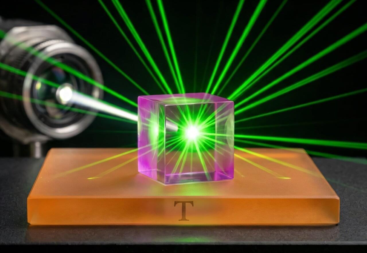
Scientists have unveiled a technique that uses ‘molecular antennas’ to direct electrical energy into insulating nanoparticles. This approach creates a new family of ultra-pure near-infrared LEDs that could be used in medical diagnostics, optical communication systems, and sensitive detectors.

Researchers at the Cavendish Laboratory, University of Cambridge have discovered how to drive electrical current into materials that normally do not conduct, a feat previously thought impossible under normal conditions. By attaching carefully chosen organic molecules that act like tiny antennas, they have built the first light-emitting diodes (LEDs) from insulating nanoparticles. Their work, reported in Nature, points toward a new generation of devices for deep-tissue biomedical imaging and high-speed data transmission.

/* */