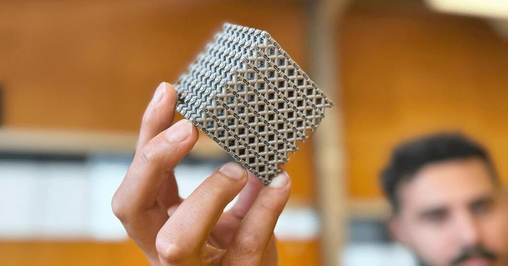
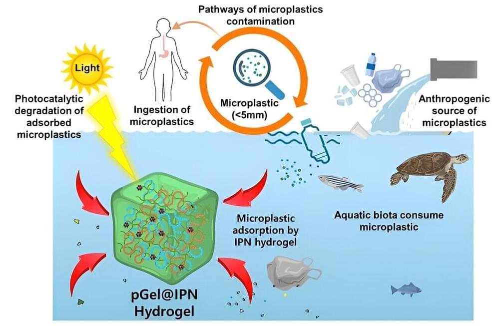
Toggle light / dark theme

Dracula’s Chivito: New Protoplanetary Disk discovered with Pan-STARRS

A protoplanetary disk is a disk of dense gas and dust, orbiting a newly formed star. It is assumed that planets are born by the gradual accumulation of material in such a structure, therefore discoveries and studies of protoplanetary disks are essential for improving our understanding of planetary formation processes.

Now, a team of astronomers led by Ciprian T. Berghea of the U.S. Naval Observatory (USNO) in Washington, DC, has discovered a new disk of this type that is associated with an infrared source known as IRAS 23077+6707. The finding was made by inspecting the Pan-STARRS data while working on a variability study of active galactic nuclei (AGN) candidates.

Percutaneous Continuous Radiofrequency Versus Pulsed Radiofrequency Thermorhizotomy for the Treatment of Neuralgia of the Trigeminal Nerve: A Retrospective Observational Study

Objectives: Trigeminal neuralgia (TN) represents one of the most powerful manifestations of neuropathic pain. The diagnostic criteria, as well as its therapeutic modalities, stand firmly established. The percutaneous radiofrequency thermorhizotomy of the gasserian ganglion and posterior root of the trigeminal nerve stands as a widely employed procedure in this context. In this retrospective observational investigation, we undertake a comparative analysis of patients subjected to treatment employing continuous radiofrequency (C-rF) versus pulsed radiofrequency (P-rF).

Materials and methods: A cohort of 128 patients afflicted with essential neuralgia of the trigeminal nerve, all under the care of the distinguished author (JCA), underwent percutaneous radiofrequency thermorhizotomy between the years 2005 and 2022. They were stratified into two cohorts: Group 1 encompassed 76 patients treated with C-rF, while Group 2 comprised 52 patients subjected to P-rF intervention. All participants met the stringent inclusion and exclusion criteria for TN, with a notable concentration in the V2 and V3 territories accounting for 60% and 45%, respectively. The post-procedural follow-up period exhibited uniformity, spanning from six months to 16 years. Preceding the intervention, all patients uniformly reported a visual analog scale (VAS) score surpassing 6/10. Additionally, everyone had been undergoing pharmacological management, involving a combination of antineuropathic agents and low-potency opioids.

Results: The evaluation of clinical improvement was conducted across three temporal domains: the immediate short-term (less than 30 days), the intermediate-term (less than one year), and the prolonged-term (exceeding one year). In the short term, a noteworthy alleviation of pain, surpassing the 50% threshold, was evident in most patients (94%), a similarity observed in both cohorts (98% in Group 1 and 90% in Group 2). The VAS revealed an average rating of 3/10 for Group 1 and 2/10 for Group 2. Moving to the intermediate term, more than 50% improvement in pain was registered in 89% of patients (92% in Group 1 and 86% in Group 2). The mean VAS score stood at 3.5÷10, marginally higher in Group 2 at 4/10 compared to 3/10 in Group 1. In the final assessment, a 50% or greater reduction in pain was reported by 75% of patients, with no discernible disparity between the two cohorts. Among the cohort, 18 individuals necessitated a subsequent percutaneous intervention (10 in Group 1 and eight in Group 2), while microvascular decompression was performed on six patients (equitably distributed between the two groups), and radiosurgery was administered to three patients in Group 1.

Breakthrough Pseudo CMOS Transistors for 1000 Times More Efficient Computing

Beijing researchers made a pseudo-CMOS architecture for sub-picowatt logic computing that uses self-biased molybdenum disulfide transistors.

As transistors are scaled to smaller dimensions, their static power increases. Combining two-dimensional (2D) channel materials with complementary metal–oxide–semiconductor (CMOS) logic architectures could be an effective solution to this issue because of the excellent field-effect properties of 2D materials. However, 2D materials have limited polarity control. The transistors have a gapped channel that forms a tunable barrier—thus circumventing the polarity control of 2D materials—and exhibit a reverse-saturation current below 1 pA with high reliability and endurance.

They use the devices to make homojunction-loaded inverters with good rail-to-rail operation at a switching threshold voltage of around 0.5 V, a static power of a few picowatts, a dynamic delay time of around 200 µs, a noise margin of more than 90% and a peak voltage gain of 241. They also fabricate fundamental gate circuits on the basis of this pseudo-CMOS configuration by cascading several devices.

Surface Acoustic Wave Cavity Optomechanics with Atomically Thin $h$-BN and mathrmWSe_2$ Single-Photon Emitters

In pursuing quantum networking technologies, single-photon emitters in acoustic cavities are a promising pathway that enables the conversion and transfer of quantum information across multiple platforms. The recent discovery of single-photon emitters within two-dimensional (2D) materials, such as WSe and hexagonal boron nitride (h-BN), opens new avenues in exploring such quantum optomechanical phenomena in lower dimensional systems. In this work, we demonstrate the integration of 2D-based single-photon emitters with surface acoustic wave optomechanical cavities and illustrate their potential for radio-frequency electronic control of quantum light emission.

Using simple exfoliation techniques, WSe and h-BN layers are transferred onto surface acoustic wave cavities patterned on lithium niobate—a highly piezoelectric host material. Using electro-optical measurements, we confirm high-quality resonators and cavity-phonon modes that couple to the 2D quantum emitters. Remarkably, the interaction between the 2D emitters and acoustic waves is exceptionally strong owing to the ultrathin nature of the 2D materials and their proximity to the surface waves, verified through quantum spectroscopy measurements. In addition to the radio-frequency acoustic modulation of the emitters in these materials, new physics emerges from the emitter-phonon coupling that leads to new mechanisms for high-speed manipulation of quantum emitters, opening avenues for the generation of entangled-photon pairs.

These advancements set the stage for the exploration of cavity optomechanics with 2D materials. In future experiments, higher frequency resonators will enable studies of the interplay and dynamics between single photons and phonons deep in the quantum regime, a key technology for quantum networking.

Orbital Magic: Japanese Scientists Pave the Way for Next-Gen Spintronics

Directing magnetization with a low electric field is crucial for advancing effective spintronic devices. In spintronics, the characteristics of an electron’s spin or magnetic moment are leveraged for information storage. By modifying orbital magnetic moments through strain, it’s possible to manipulate electron spins, leading to an enhanced magnetoelectric effect for superior performance.

Japanese researchers, including Jun Okabayashi from the University of Tokyo, revealed a strain-induced orbital control mechanism in interfacial multiferroics. In multiferroic material, the magnetic property can be controlled using an electric field—potentially leading to efficient spintronic devices. The interfacial multiferroics that Okabayashi and his colleagues studied consist of a junction between a ferromagnetic material and a piezoelectric material. The direction of magnetization in the material could be controlled by applying voltage.

Spintronics research finds magnetic state of certain materials can be switched using surface induced strain

Electronics are based on electrical charges being transported from one place to another. Electrons move, current flows, and signals are transmitted by applying an electrical voltage. However, there is also another way to manipulate electronic currents and signals: using the properties of the spin—the intrinsic magnetic moment of the electron. This is called “spintronics,” and it has become an increasingly important field in contemporary electronic research.

An international research team involving TU Wien and the Czech Academy of Sciences has now achieved an important breakthrough. They have managed to switch the spins in an antiferromagnetic material using surface strain. This could lead to an important new line of research in electronic technologies. The research is published in the journal Advanced Functional Materials.

“There are different types of magnetism,” explains Sergii Khmelevskyi from the Vienna Scientific Cluster Research Center, TU Wien. “The best known is ferromagnetism. It occurs when the atomic spins in a material are all aligned in parallel. But there is also the opposite, antiferromagnetism. In an antiferromagnetic material, neighboring atoms always have opposite spins.” Their effects therefore cancel each other out and no can be detected from the outside.

/* */