It’s a bit harder to replace than a stolen credit card if something goes wrong, though.


Physicists at LMU have developed a highly sensitive method for measuring the mechanical stability of protein conformations, and used it to monitor the early steps in the formation of blood clots.
As the central mediators of cell function in biological organisms, proteins are involved in the execution of virtually all cellular processes. They provide the internal scaffolding that gives cells their form, and enable cells to dynamically alter their morphology. They transport substrates back and forth across membranes, and they catalyze most of the chemical reactions that take place in cells. In the course of these tasks many proteins are subjected to external forces. Indeed, some “mechanosensitive” proteins effectively measure the strength of the forces acting upon them and are activated when the imposed force exceeds a given threshold value. Von Willebrand Factor (VWF), which initiates the formation of blood clots, is an important representative of this class.
The mechanical forces required to activate proteins like VWF are often so small that their magnitude could not be determined using existing methods. Now, a team of scientists led by LMU physicists Dr. Martin Benoit and Professor Jan Lipfert has developed a much more sensitive procedure. Their “magnetic tweezers” can quantify forces that are 100 times smaller than the commonly used alternative method currently available. As Lipfert and colleagues report in the journal PNAS, they have employed the technique to observe the unfolding of the VWF protein under the influence of low mechanical forces.

Former NASA engineer and Bitcoin advocate Beth Moses says she got a birds-eye view of humanity from outer space when she became the world’s first woman commercial astronaut earlier this year. Part of a three-person flight team, Moses soared 55.87 miles (89.9 kilometers) into orbit as a “test passenger” aboard Virgin Galactic’s second spaceflight on February 22.
An early proponent of Bitcoin, she began mining BTC after she read Satoshi Nakamoto’s white paper in 2013. As Virgin Galactic’s chief astronaut instructor and interiors program manager, Moses believes global tools can solve critical problems.
Says Moses, in a recent report by Forbes.

NBC is developing an untitled cryonics-themed project which hails from writer and executive producer David Slack and filmmaker Phillip Noyce who will direct the pilot and executive produce.
Sony Television produces the series which follows an enigmatic billionaire who has gathered more than 250 people who attempt to cheat death by undergoing cryogenic suspension in hopes that a future breakthrough would someday allow them to be brought back to life.
However, as these people from different moments in time wake up, they soon realise you can’t cheat death without paying a price. Josh Berman and Chris King will also serve as executive producer. Noyce also helmed the pilots of and executive produced ABC’s “Revenge” and FOX’s “The Resident”.

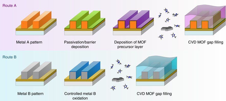
Researchers at KU Leuven and imec have successfully developed a new technique to insulate microchips. The technique uses metal-organic frameworks, a new type of materials consisting of structured nanopores. In the long term, this method can be used for the development of even smaller and more powerful chips that consume less energy. The team has received an ERC Proof of Concept grant to further their research.
Computer chips are getting increasingly smaller. That’s not new: Gordon Moore, one of the founders of chip manufacturer Intel, already predicted it in 1965. Moore’s law states that the number of transistors in a chip, or integrated circuit, doubles about every two years. This prognosis was later adjusted to 18 months, but the theory still stands. Chips are getting smaller and their processing power is increasing. Nowadays, a chip can have over a billion transistors.
But this continued reduction in size also brings with it a number of obstacles. The switches and wires are packed together so tightly that they generate more resistance. This, in turn, causes the chip to consume more energy to send signals. To have a well-functioning chip, you need an insulating substance that separates the wires from each other, and ensures that the electrical signals are not disrupted. However, that’s not an easy thing to achieve at the nanoscale level.

Light-emitting diodes made of indium gallium nitride provide better luminescence efficiency than many of the other materials used to create blue and green LEDs. But a big challenge of working with InGaN is its known dislocation density defects that make it difficult to understand its emission properties.
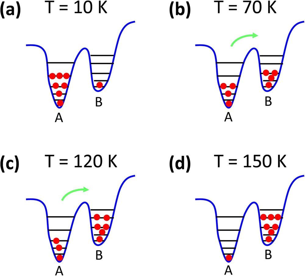
In the Journal of Applied Physics, researchers in China report an InGaN LED structure with high luminescence efficiency and what is believed to be the first direct observation of transition carriers between different localization states within InGaN. The localization states were confirmed by temperature-dependent photoluminescence and excitation power-dependent photoluminescence.
Localization states theory is commonly used to explain the high luminescence efficiency gained via the large number of dislocations within InGaN materials. Localization states are the energy minima states believed to exist within the InGaN quantum well region (discrete energy values), but a direct observation of localization states was elusive until now.