Apple says the iPhone 11 and iPhone 11 Pro feature the “toughest glass in a smartphone” and yesterday we saw the first drop test videos emerge. Now, PhoneBuff has shared a new video pitting the durability of the iPhone 11 Pro Max vs the Galaxy Note 10+.
Category: mobile phones – Page 194
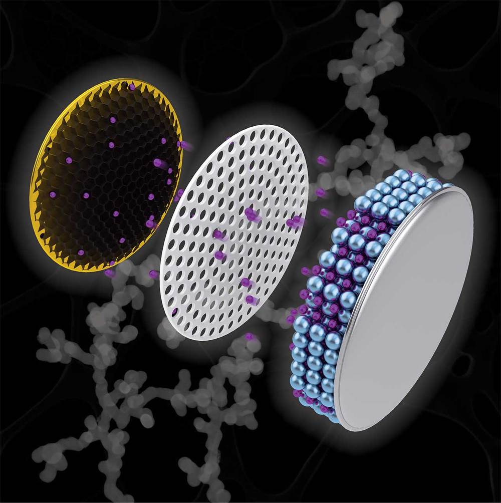
Nanochains could increase battery runtime and speed charging
Researchers at Purdue University have announced a breakthrough that could have a significant impact on batteries of the future. The team says that the runtime for the battery in a phone or computer depends on how many lithium-ions can be stored in the negative electrode material inside the battery. When those ions are depleted, the battery is unable to deliver an electrical current.

‘Nanochains’ could increase battery capacity, cut charging time
How long the battery of your phone or computer lasts depends on how many lithium ions can be stored in the battery’s negative electrode material. If the battery runs out of these ions, it can’t generate an electrical current to run a device and ultimately fails.
Materials with a higher lithium ion storage capacity are either too heavy or the wrong shape to replace graphite, the electrode material currently used in today’s batteries.
Purdue University scientists and engineers have introduced a potential way that these materials could be restructured into a new electrode design that would allow them to increase a battery’s lifespan, make it more stable and shorten its charging time.

Researchers Think It’s a Good Idea to Secure Your Phone Using the One Thing You Perpetually Lose
Apple’s FaceID authentication system started moving smartphone users away from relying on fingerprints to secure their mobile devices, which are arguably less secure. But researchers think they’ve come up with an even better biometric tool for protecting a device that uses a part of the body that’s nearly impossible to spoof: a user’s ear canals.
A team of researchers led by Zhanpeng Jin, an associate professor in the Department of Computer Science and Engineering in the University of Buffalo’s School of Engineering and Applied Sciences, created a new authentication tool called EarEcho, which is somewhat self-explanatory. The team modified a set of off the shelf earbuds with a tiny microphone that points inside the wearer’s ear, not out towards the world around them. It’s not there to pick up ambient sounds to facilitate a noise-canceling or feature, or even the wearer’s voice for making calls; the tiny mic is instead tuned to listen to the echo of sounds as they’re played and then propagate through the ear canal.
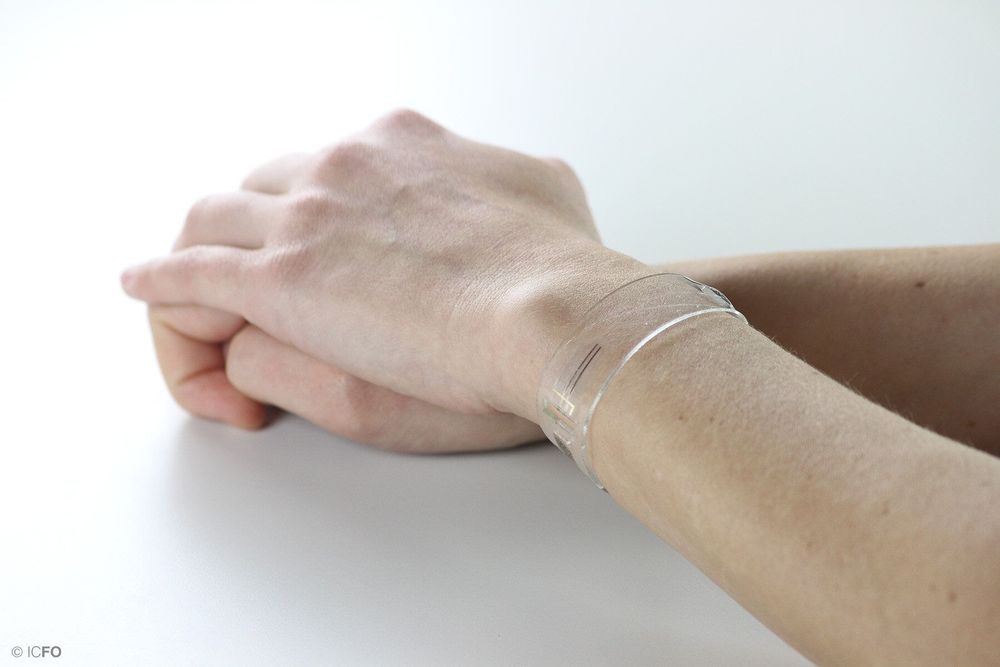
New health monitors are flexible, transparent and graphene enabled
New technological devices are prioritizing non-invasive tracking of vital signs, not only for fitness monitoring, but also for the prevention of common health problems such as heart failure, hypertension and stress-related complications, among others. Wearables based on optical detection mechanisms are proving an invaluable approach for reporting on our bodies inner workings and have experienced a large penetration into the consumer market in recent years. Current wearable technologies, based on non-flexible components, do not deliver the desired accuracy and can only monitor a limited number of vital signs. To tackle this problem, conformable non-invasive optical-based sensors that can measure a broader set of vital signs are at the top of the end-users’ wish list.
In a recent study published in Science Advances, ICFO researchers have demonstrated a new class of flexible and transparent wearable devices that are conformable to the skin and can provide continuous and accurate measurements of multiple human vital signs. These devices can measure heart rate, respiration rate and blood pulse oxygenation, as well as exposure to UV radiation from the sun. While the device measures the different parameters, the read-out is visualized and stored on a mobile phone interface connected to the wearable via Bluetooth. In addition, the device can operate battery-free since it is charged wirelessly through the phone.
“It was very important for us to demonstrate the wide range of potential applications for our advanced light sensing technology through the creation of various prototypes, including the flexible and transparent bracelet, the health patch integrated on a mobile phone and the UV monitoring patch for sun exposure. They have shown to be versatile and efficient due to these unique features,” reports Dr. Emre Ozan Polat, first author of this publication.
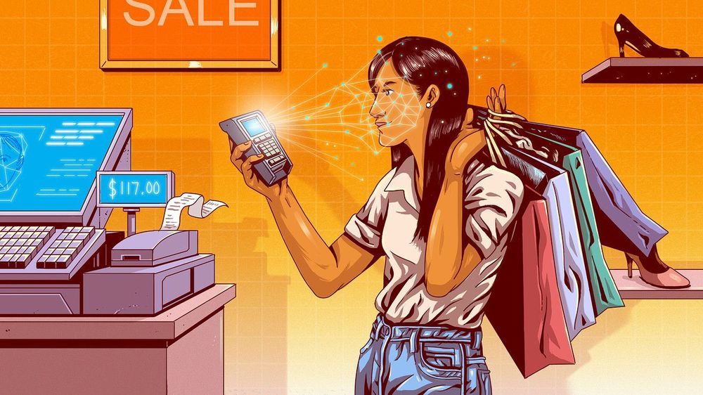
Silicon Valley’s final frontier for mobile payments — ‘the neoliberal takeover of the human body’
Biometric mobile wallets — payment technologies using our faces, fingerprints or retinas — already exist. Notable technology companies including Apple AAPL, +2.62% and Amazon AMZN, +0.26% await a day when a critical mass of consumers is sufficiently comfortable walking into a store and paying for goods without a card or device, according to Sinnreich, author of “The Essential Guide to Intellectual Property.”
Removing the last physical barrier — smartphones, watches, smart glasses and credit cards — between our bodies and corporate America is the final frontier in mobile payments. “The deeper the tie between the human body and the financial networks, the fewer intimate spaces will be left unconnected to those networks,” Sinnreich said.
The internet’s second revolution | The Economist
The second half of humanity is joining the internet. People in countries like India will change the internet, and it will change them. Read more from The Economist here: https://econ.st/2zVWeQQ
Click here to subscribe to The Economist on YouTube: https://econ.st/2xvTKdy
L.O. Two simple letters that marked one of the biggest changes in human history. In 1969 programmers were trying to type “login”.
50 years later and half the world is now online. But that half is primarily from the rich world. How will the second half of humanity coming online change the internet and how will the internet change them?
India’s internet penetration was pretty low until very recently with the launch of a new mobile network called Reliance Jio, with incredibly cheap phones and incredibly cheap data prices. Reliance Jio launched aggressively in 2016 offering subsidised handsets and free data to hook people in. India went from being a relatively expensive place to consume data to being the cheapest in the world. Prices crashed by 94%
Newer users in the developing world are browsing the internet in much the same way as people in the developed world.
“Infinite” Energy Storage Finally Discovered, But There’s A Catch
The Intertubes have been buzzing with news that a research team based at UC-Irvine has created a new type of energy storage device that can last for more than 100,000 charges. For all practical purposes, that counts as an infinite battery. Under real life conditions, such a battery would most likely outlive the device it powers, and it might even outlive the owner of the device as well.
The new battery is still in the early research stage, but if it pans out, it would have a significant impact on lifecycle and supply chain issues for the ballooning number of smart phones, electric vehicles, energy storage products, and countless other battery powered devices inhabiting the Earth.
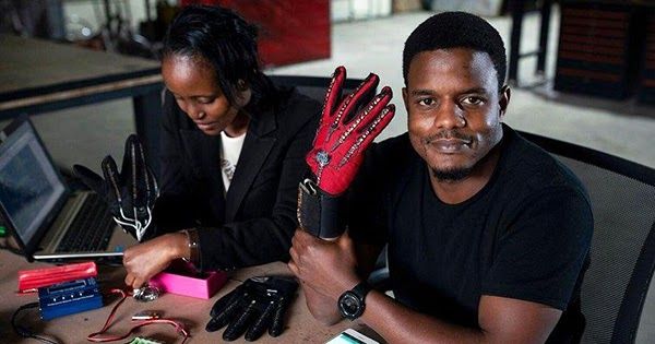
Black Engineer Invents Gloves That Turn Sign Language into Audible Speech
Shouldn’t the title just be “Engineer”? What an amazing product!
Roy Allela, a 25-year old engineer and inventor from Kenya, has found the ultimate solution to bridging the communication barrier between deaf and hearing people. He has invented the Sign-IO gloves that can translate signed hand movements to audible speech so deaf people can “talk” even to those who don’t understand sign language.
The Sign-IO gloves feature sensors mounted on each of the five fingers to determine its movements, including how much a finger is bent. The gloves are connected via Bluetooth to an Android app that Allela also invented which uses a text-to-speech function to convert the gestures to vocal speech.
Allela was inspired to create the gloves because he and his family struggled to communicate with his 6-year-old niece who was born deaf. “My niece wears the gloves, pairs them to her phone or mine, then starts signing and I’m able to understand what she’s saying. Like all sign language users, she’s very good at lip reading, so she doesn’t need me to sign back,” he said in an interview with The Guardian.