This is according to a report by the institution published on Tuesday.
The strongest material ever known
“For the given density, our material is the strongest known,” said Seok-Woo Lee, a materials scientist at UConn.

This is according to a report by the institution published on Tuesday.
The strongest material ever known
“For the given density, our material is the strongest known,” said Seok-Woo Lee, a materials scientist at UConn.
YouTube.
But in a development that is creating a lot of buzz, and at the same time a bit of suspicion from the scientific community, a team of Korean researchers have claimed that they have created a superconductor capable of conducting electricity perfectly at room temperature and ambient pressure.

The world’s largest community of 3D-printed homes is being built in Texas — and the neighborhood just unveiled its first completed house.
With walls “printed” using a concrete-based material, the single-story structure is the first of 100 such homes set to welcome residents starting September.
The community is part of a wider development in Georgetown, Texas called Wolf Ranch. It’s located about 30 miles north of Austin, the state capital, and is a collaboration between Texas construction firm ICON, homebuilding company Lennar and Danish architecture practice Bjarke Ingels Group (BIG).

Black holes are the most mysterious objects in the universe, with features that sound like they come straight from a sci-fi movie.
Stellar-mass black holes with masses of roughly 10 suns, for example, reveal their existence by eating materials from their companion stars. And in some instances, supermassive black holes accumulate at the center of some galaxies to form bright compact regions known as quasars with masses equal to millions to billions of our sun. A subset of accreting stellar-mass black holes that can launch jets of highly magnetized plasma are called microquasars.
An international team of scientists, including UNLV astrophysicist Bing Zhang, reports in Nature on a dedicated observational campaign on the galactic microquasar dubbed GRS 1915+105. The team revealed features of a microquasar system that have never before been seen.

In today’s world of digital information, an enormous amount of data is exchanged and stored on a daily basis.
In the 1980s, IBM unveiled the first hard drive—which was the size of a refrigerator—that could store 1 GB of data, but now we have memory devices that have a thousand-fold greater data-storage capacity and can easily fit in the palm of our hand. If the current pace of increase in digital information is any indication, we require yet newer data recording systems that are lighter, have low environmental impact, and, most importantly, have higher data storage density.
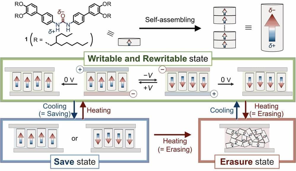
Recently, a new class of materials called axially polar-ferroelectric columnar liquid crystals (AP-FCLCs) has emerged as a candidate for future high-density memory storage materials. An AP-FCLC is a liquid crystal with a structure of parallel columns generated by molecular self-assembly, which have polarization along the column axis.


Mysterious radio wave pulses from deep in space have been hitting Earth for decades, but the scientists who recently discovered them have no concrete explanation for the origin of the signals.
For 35 years, the strange blasts of energy in varying levels of brightness have occurred like clockwork approximately every 20 minutes, sometimes lasting for five minute intervals. That’s what Curtin University astronomers from the International Centre for Radio Astronomy Research (ICRAR) concluded in research published last week in the journal Nature.
The discovery of the signal, which researchers named GPMJ1839-10, has the scientists baffled. Believed to be coming from around 15,000 light years away from Earth, the signal has been occurring at intervals and for a period of time previously thought to be impossible.

Materials that are both strong and lightweight could improve everything from cars to body armor. But usually, the two qualities are mutually exclusive. Now, University of Connecticut researchers and colleagues have developed an extraordinarily strong, lightweight material using two unlikely building blocks: DNA and glass.
“For the given density, our material is the strongest known,” says Seok-Woo Lee, a materials scientist at UConn. Lee and colleagues from UConn, Columbia University, and Brookhaven National Lab report the details on July 19 in Cell Reports Physical Science.
Strength is relative. Iron, for example, can take 7 tons of pressure per square centimeter. But it’s also very dense and heavy, weighing 7.8 grams/cubic centimeter. Other metals, such as titanium, are stronger and lighter than iron. And certain alloys combining multiple elements are even stronger. Strong, lightweight materials have allowed for lightweight body armor, better medical devices and made safer, faster cars and airplanes. The easiest way to extend the range of an electric vehicle, for example, is not to enlarge the battery but rather make the vehicle itself lighter without sacrificing safety and lifetime. But traditional metallurgical techniques have reached a limit in recent years, and materials scientists have had to get even more creative to develop new lightweight high strength materials.

It turns out there’s a lot of scrap wood produced by the US Army. According to the US Army Corps of Engineers, more than 80 percent of solid waste produced at the Department of Defense (DoD) forward operating bases consists of scrap wood, cardboard, and paper. This equates to almost 13 pounds of waste per soldier per day that could be reused if handled properly, reducing garbage and supplying useful materials for construction.
DARPA’s new Waste Upcycling for Defense (WUD) program aims to produce a process for turning scrap wood, cardboard, and paper into lightweight, strong, and sustainable materials for reuse in a variety of DoD environments.
