Scientist says the material has a reflectivity of 104% in the visible region which is obtained by the photoluminescence effect.
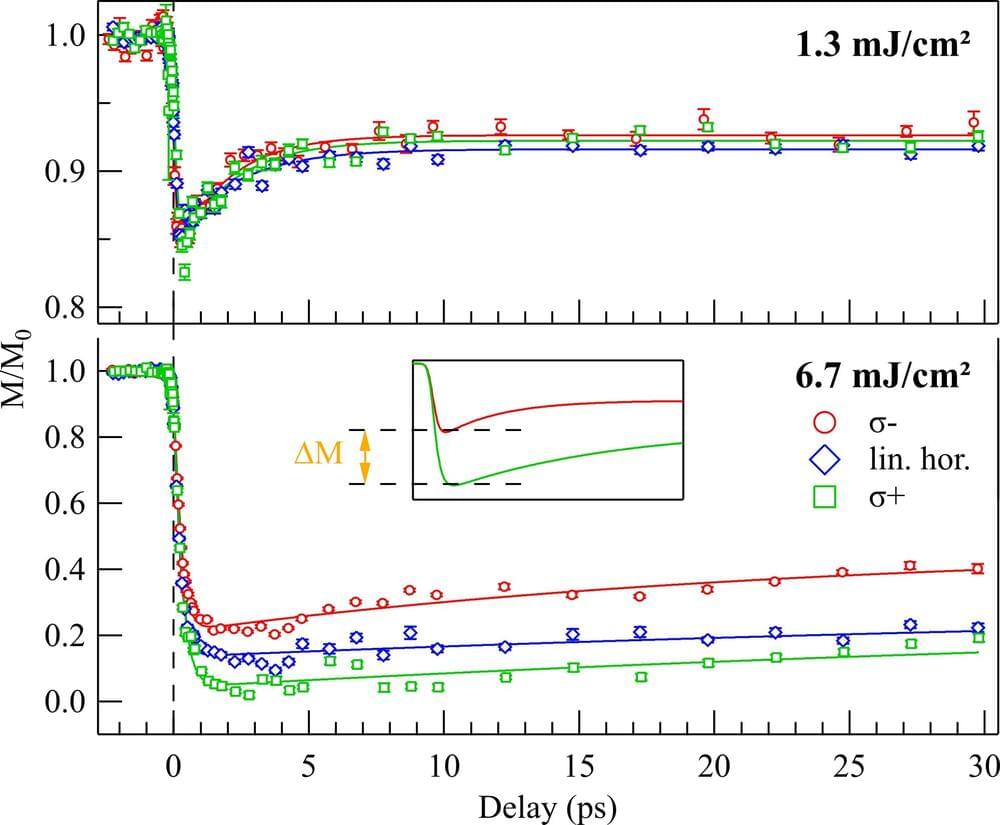
Intense laser pulses can be used to manipulate or even switch the magnetization orientation of a material on extremely short time scales. Typically, such effects are thermally induced, as the absorbed laser energy heats up the material very rapidly, causing an ultrafast perturbation of the magnetic order.
Scientists from the Max Born Institute (MBI), in collaboration with an international team of researchers, have now demonstrated an effective non-thermal approach of generating large magnetization changes.
By exposing a ferrimagnetic iron-gadolinium alloy to circularly polarized pulses of extreme ultraviolet (XUV) radiation, they could reveal a particularly strong magnetic response depending on the handedness of the incoming XUV light burst (left-or right-circular polarization).

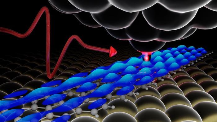
One of the challenges of cramming smarter and more powerful electronics into ever-shrinking devices is developing the tools and techniques to analyze the materials that make them up with increasingly intimate precision.
Physicists at Michigan State University have taken a long-awaited step on that front with an approach that combines high-resolution microscopy with ultrafast lasers.
The technique, described in the journal Nature Photonics, enables researchers to spot misfit atoms in semiconductors with unparalleled precision. Semiconductor physics labels these atoms as “defects,” which sounds negative, but they’re usually added to materials on purpose and are critically important to the performance of semiconductors in today’s—and tomorrow’s—devices.

One of the challenges of cramming smarter and more powerful electronics into ever-shrinking devices is developing the tools and techniques to analyze the materials that make them up with increasingly intimate precision.
Physicists at Michigan State University have taken a long-awaited step on that front with an approach that combines high-resolution microscopy with ultrafast lasers.
The technique, described in the journal Nature Photonics (“Atomic-scale terahertz time-domain spectroscopy”), enables researchers to spot misfit atoms in semiconductors with unparalleled precision. Semiconductor physics labels these atoms as “defects,” which sounds negative, but they’re usually added to materials on purpose and are critically important to the performance of semiconductors in today’s — and tomorrow’s — devices.
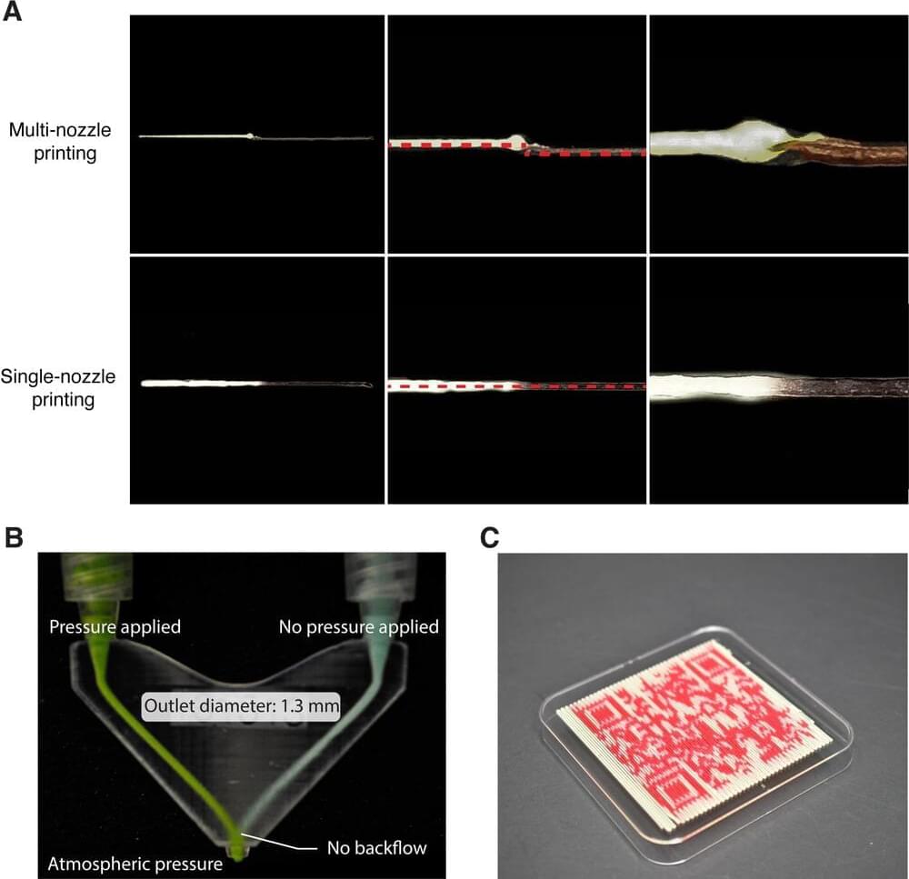
Like a scene from the movies, a team of researchers from Singapore University of Technology and Design (SUTD) has developed new ways to freely produce and customize the food that we eat.
Their findings have been published in the journal Future Foods as “Multi-material direct ink writing 3D food printing using multi-channel nozzle.”
Three-dimensional (3D) printing using food ingredients is currently the favored approach to shaping foods with unique structures, textures, and nutritional compositions.
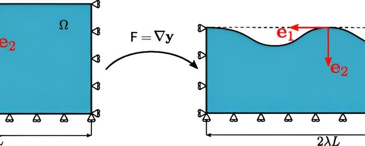
A new theory has finally deciphered the physical mechanisms of fracture in soft materials. This discovery could soon lead to new, defect-free materials that are more resistant and durable as well as environmentally friendly. The article “Elastic instability behind brittle fracture” was recently published by Physical Review Letters.
“We have revealed that fracture propagates from the free surface of the material, starting from an elastic instability that breaks the symmetry of the object. Then, the rupture drastically extends with an intricate network of cracks spreading like a turbulence phenomenon similar to what we observe in fluids, like during vortex formation,” explains Pasquale Ciarletta from the MOX Laboratory, Department of Mathematics at Politecnico di Milano.
This discovery stimulates significant applications in various technological sectors. For instance, in the production of micro and nano devices, where materials need to be extremely resistant and defect-free.
A groundbreaking study has demonstrated the use of liquid crystals for efficient and tunable spontaneous parametric down-conversion (SPDC), expanding the potential of quantum light sources beyond traditional solid materials.
Spontaneous parametric down-conversion (SPDC), a key method for generating entangled photons used in quantum physics and technology, has traditionally been restricted to solid materials. However, researchers at the Max Planck Institute for the Science of Light (MPL) and the Jozef Stefan Institute in Ljubljana, Slovenia, have recently achieved a breakthrough by demonstrating SPDC in a liquid crystal for the first time. Their findings, published in Nature, pave the way for the development of a new generation of quantum sources that are both efficient and tunable by electric fields.
The splitting of a single photon in two is one of the most useful tools in quantum photonics. It can create entangled photon pairs, single photons, squeezed light, and even more complicated states of light which are essential for optical quantum technologies. This process is known as spontaneous parametric down-conversion (SPDC).


To take a picture, the best digital cameras on the market open their shutter for around around one four-thousandths of a second.
To snapshot atomic activity, you’d need a shutter that clicks a lot faster.
With that in mind, scientists have unveiled a way of achieving a shutter speed that’s a mere trillionth of a second, or 250 million times faster than those digital cameras. That makes it capable of capturing something very important in materials science: dynamic disorder.