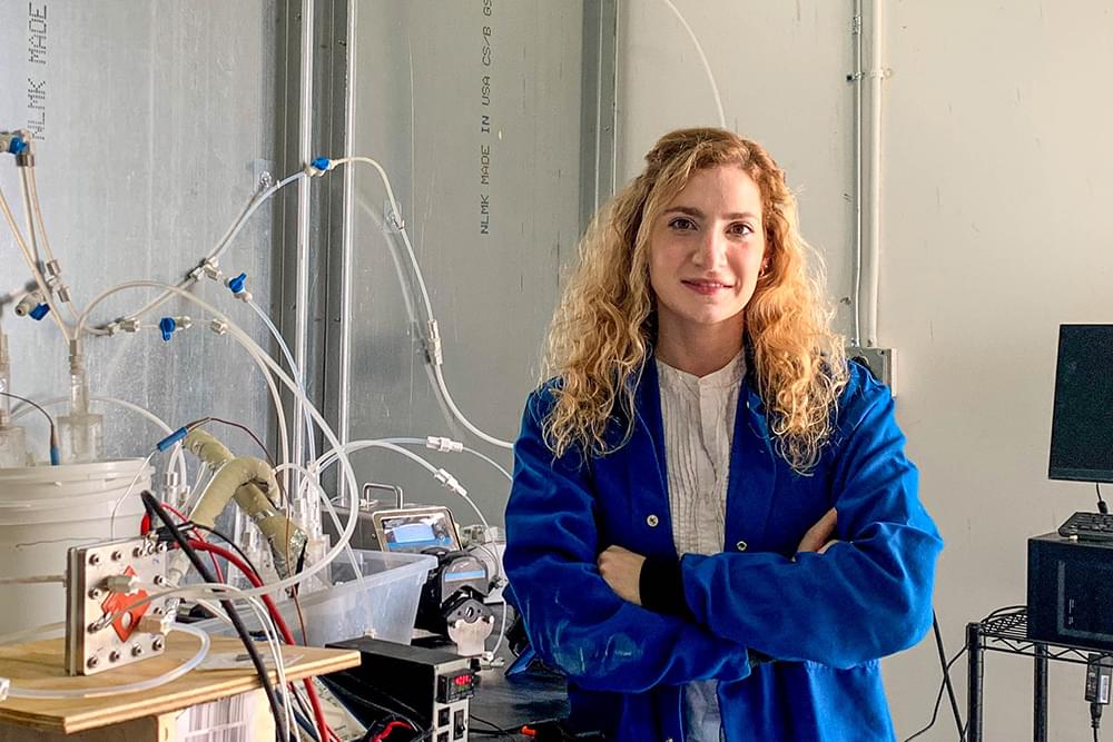
“If we’re going to use scrap aluminum for hydrogen generation in a practical application, we need to be able to better predict what hydrogen generation characteristics we’re going to observe from the aluminum-water reaction,” says Laureen Meroueh PhD ’20, who earned her doctorate in mechanical engineering.
Since the fundamental steps in the reaction aren’t well understood, it’s been hard to predict the rate and volume at which hydrogen forms from scrap aluminum, which can contain varying types and concentrations of alloying elements. So Hart, Meroueh, and Thomas W. Eagar, a professor of materials engineering and engineering management in the MIT Department of Materials Science and Engineering, decided to examine — in a systematic fashion — the impacts of those alloying elements on the aluminum-water reaction and on a promising technique for preventing the formation of the interfering oxide layer.
To prepare, they had experts at Novelis Inc. fabricate samples of pure aluminum and of specific aluminum alloys made of commercially pure aluminum combined with either 0.6 percent silicon (by weight), 1 percent magnesium, or both — compositions that are typical of scrap aluminum from a variety of sources. Using those samples, the MIT researchers performed a series of tests to explore different aspects of the aluminum-water reaction.


