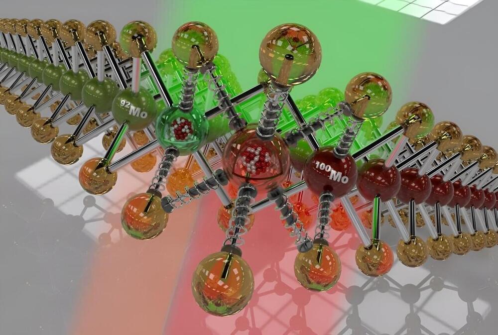
Partly because of semiconductors, electronic devices and systems become more advanced and sophisticated every day. That’s why for decades researchers have studied ways to improve semiconductor compounds to influence how they carry electrical current. One approach is to use isotopes to change the physical, chemical and technological properties of materials.
Isotopes are members of a family of an element that all have the same number of protons but different numbers of neutrons and thus different masses. Isotope engineering has traditionally focused on enhancing so-called bulk materials that have uniform properties in three dimensions, or 3D.
But new research led by ORNL has advanced the frontier of isotope engineering where current is confined in two dimensions, or 2D, inside flat crystals and where a layer is only a few atoms thick. The 2D materials are promising because their ultrathin nature could allow for precise control over their electronic properties.
