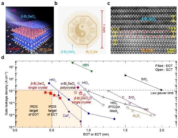
Field-effect transistors (FETs) are transistors in which the resistance of most of the electrical current can be controlled by a transverse electric field. Over the past decade or so, these devices have proved to be very valuable solutions for controlling the flow of current in semiconductors.
To further develop FETs, electronics engineers worldwide have recently been trying to reduce their size. While these down-scaling efforts have been found to increase the device’s speed and lower the power consumption, they are also associated with short-channel effects (i.e., unfavorable effects that occur when an FET’s channel length is approximately equal to the space charge regions of source and drain junctions within its substrate).
These undesirable effects, which include barrier lowering and velocity saturation, could be suppressed by using 2D semiconductor channels with high carrier mobilities and ultrathin high–k dielectrics (i.e., materials with high dielectric constants). Integrating 2D semiconductors with dielectrics with similar oxide thicknesses has been found to be highly challenging.
