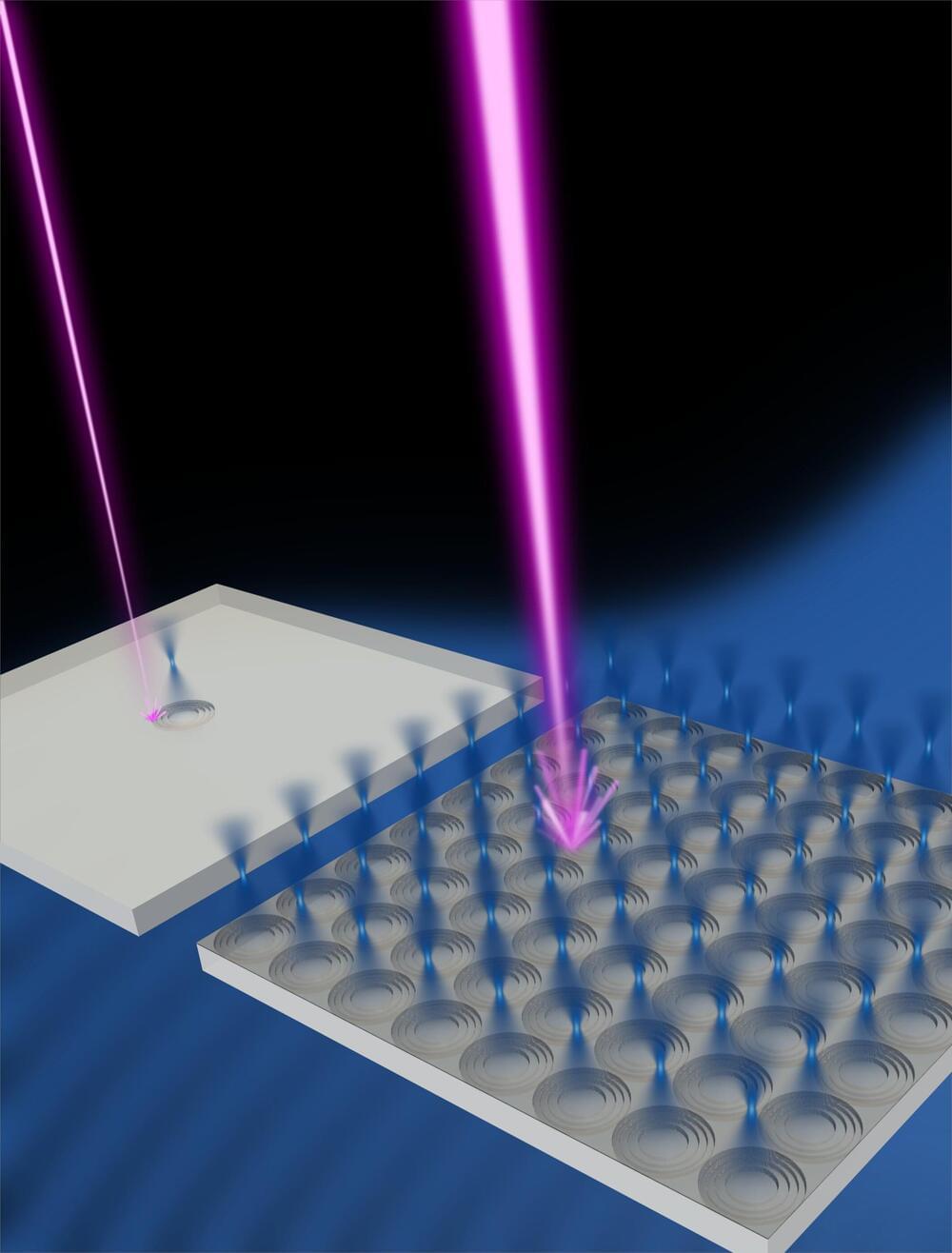
Cutting intricate patterns as small as several billionths of a meter deep and wide, the focused ion beam (FIB) is an essential tool for deconstructing and imaging tiny industrial parts to ensure they were fabricated correctly. When a beam of ions, typically of the heavy metal gallium, bombards the material to be machined, the ions eject atoms from the surface—a process known as milling—to sculpt the workpiece.
Beyond its traditional uses in the semiconductor industry, the FIB has also become a critical tool for fabricating prototypes of complex three-dimensional devices, ranging from lenses that focus light to conduits that channel fluid. Researchers also use the FIB to dissect biological and material samples to image their internal structure.
However, the FIB process has been limited by a trade-off between high speed and fine resolution. On the one hand, increasing the ion current allows a FIB to cut into the workpiece deeper and faster. On the other hand, the increased current carries a larger number of positively charged ions, which electrically repel each other and defocus the beam. A larger, diffuse beam, which can be about 100 nanometers in diameter or 10 times wider than a typical narrow beam, not only limits the ability to fabricate fine patterns but can also damage the workpiece at the perimeter of the milled region. As a result, the FIB has not been the process of choice for those trying to machine many tiny parts in a hurry.
