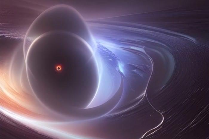
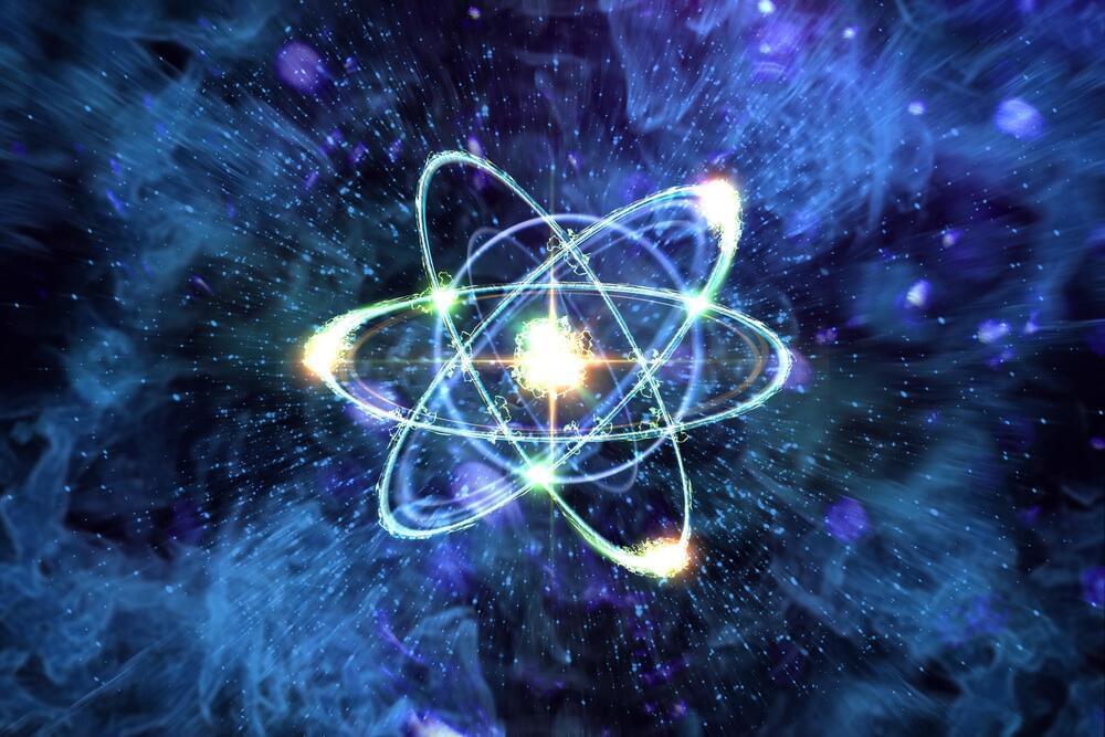
Quantum superposition is not just a property of subatomic particles but also of the most massive objects in the universe. That is the conclusion of four theoretical physicists in Australia and Canada who calculated the hypothetical response of a particle detector placed some distance from a black hole. The researchers say the detector would see novel signs of superimposed space–times, implying that the black hole may have two different masses simultaneously.
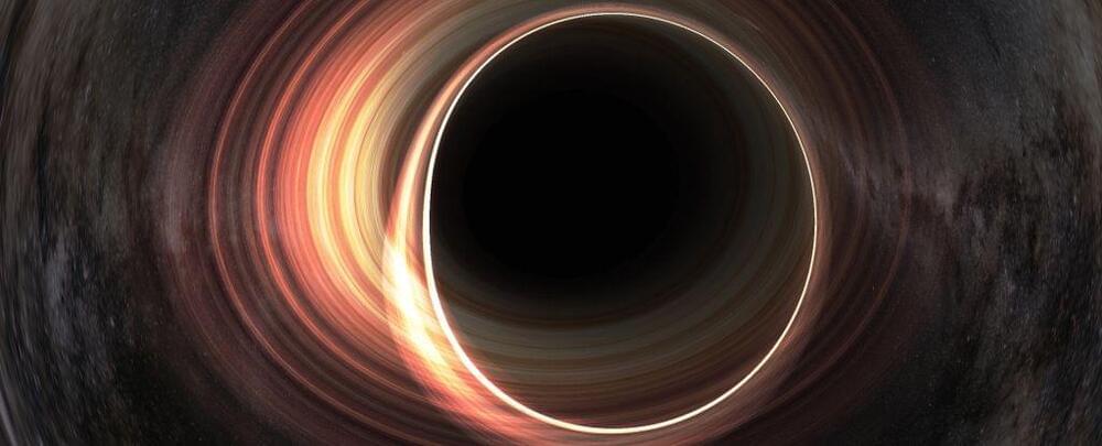
Black holes are formed when extremely massive objects like stars collapse to a singularity – a point of infinite density. The gravitational field of a black hole is so great that nothing can escape its clutches, not even light. This creates a spherical region of space around the singularity entirely cut off from the rest of the universe and bounded by what is known as an event horizon.
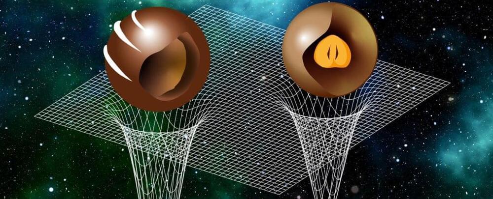
An active area of research into the physics of black holes seeks to develop a consistent theory of quantum gravity. This is an important goal of theoretical physics that would reconcile quantum mechanics and Einstein’s general theory of relativity. In particular, by considering black holes in quantum superposition, physicists hope to gain insights into the quantum nature of space–time.

