Our body contains an intricate system of tiny vessels through which blood, water and other molecules flow. When the size of the pipes shrinks to the nanoscale, where only a few molecules can fit side by side, the classical laws of physics governing the behavior of water are influenced by the atomic structure of the walls. “It’s not that classical hydrodynamics breaks down, but rather that it gets mixed with the condensed matter physics of the solid walls,” says Nikita Kavokine, tenure-track assistant professor and leader of the EPFL Quantum Plumbing Lab.
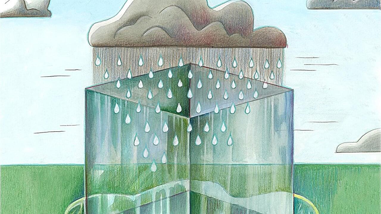
How liquids, and water in particular, behave at scales of a few nanometers is one of the big gaps in modern physics. For example, in some experiments, it has been observed that water flows through carbon nanotubes orders of magnitude faster than expected. Scientists are trying to understand phenomena that biology has mastered after millions of years of evolution.
“At the nanometer scale, our body leverages specific properties of water to filter molecules with high energy efficiency,” explains Kavokine. Aquaporins, for example, are protein channels embedded in cell membranes that use these molecular-scale interactions to let water pass while blocking ions and other molecules.