Toggle light / dark theme

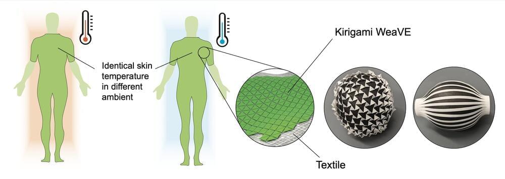
Researchers used radiative cooling to generate enough to power LEDs or charge a cell phone.


NASA has agreed to test startup SpinLaunch’s kinetic launcher, a giant circular accelerator that aims to shoot 200 kilogram satellites into space.

The California-based SpinLaunch’s launcher is located at the Spaceport America facility in New Mexico where it will carry out a test flight with NASA later this year, according to the firm.

MILLIONS of owners of the Samsung Galaxy smartphone face a security threat.

Those with an Android version 9 through 12 are at risk.

Researchers at Kryptowire published a report detailing how they discovered a serious vulnerability in the pre-installed Phone app across multiple models that could enable a hacker to take control of someone’s phone, Forbes reported.

Say cheese! Researchers have developed a tiny camera that takes amazingly clear photos. Just don’t sneeze while it’s in your hand. At the size of a coarse grain of salt, you may never find it again.

Smaller cameras could mean lighter smartphones and new James Bond–style gadgets. But that’s not all. Cameras on this scale could swim through the body, hitch a ride on an insect, scope out your brain or monitor hostile environments. And those are just a few of the possibilities.

How do you pack that much picture-taking power into something the size of a crumb? It takes a “radically different approach” to making a camera lens, says Felix Heide. He’s a computer scientist at Princeton University in New Jersey. His lab developed the camera with colleagues from the University of Washington in Seattle. The team shared its work in Nature Communications in November.

Remember He Jiankui, the Chinese scientist who shocked the world when it emerged in late 2018 that he had used CRISPR to tinker with the genetic code of IVF embryos, leading to the birth of twins who are likely the world’s first genetically modified humans?

The news led to a broad outcry among scientists, ethicists and regulators, not the least because experts in the field later found the experiment to be tainted by “egregious scientific and ethical lapses.”

Long story shot, China ended up imprisoning He, who also lost his research position at the Southern University of Science and Technology in China — but now MIT Technology Review, which first broke the news of the experiment back in 2018, reports that he’s out of prison and even answered his cell phone for a brief call.

Standard image sensors, like the billion or so already installed in practically every smartphone in use today, capture light intensity and color. Relying on common, off-the-shelf sensor technology—known as CMOS—these cameras have grown smaller and more powerful by the year and now offer tens-of-megapixels resolution. But they’ve still seen in only two dimensions, capturing images that are flat, like a drawing—until now.

Researchers at Stanford University have created a new approach that allows standard image sensors to see in three dimensions. That is, these common cameras could soon be used to measure the distance to objects.

The engineering possibilities are dramatic. Measuring distance between objects with light is currently possible only with specialized and expensive —short for “light detection and ranging”—systems. If you’ve seen a self-driving car tooling around, you can spot it right off by the hunchback of technology mounted to the roof. Most of that gear is the car’s lidar crash-avoidance system, which uses lasers to determine distances between objects.

Mojo Vision said it has created a new prototype of its Mojo Lens augmented reality contact lenses. This smart contact lens will bring “invisible computing” to life, the company believes.

The Mojo Lens prototype is a critical milestone for the company in its development, testing, and validation process, and is an innovation positioned at the intersection of smartphones, augmented reality/virtual reality, smart wearables, and health tech.

The prototype includes numerous new hardware features and technologies embedded directly into the lens — advancing its display, communications, eye tracking, and power system.

The result is a series of specialized accessories, including a sunglass holder, a can holder, and a phone or cardholder explicitly created for the new Peugeot 308. Made using the latest HP Multi Jet Fusion 3D printing technology, the products are not just innovative but also “pleasant to the touch, light, solid and easy to use.” According to the brand, they go a long way in enhancing the car’s interior, which showcases a new generation of Peugeot’s i-Cockpit –a patented new design that revolutionizes the driver’s cockpit through advanced ergonomics, head-up digital instrument displays, and interactive touchscreen technology.

According to the brand, this is just one of the first 3D printing used at Peugeot, as the company plans to continue implementing it for more technical parts in future car models. Moreover, as part of the PSA Group, which recently merged with Fiat Chrysler Automobiles (FCA) to create Stellantis, Peugeot is now a sister company to 13 other car manufacturers, including Dodge, Jeep, and Maserati, so looking at the bigger picture, we can imagine that the use of additive manufacturing will trickle down to the other brands under the Stellantis umbrella.

An elastic light-emitting polymer that glows like a filament in a light bulb could lead to affordable, practical and robust flexible screens.

Flexible screens could form part of wearable computers that stick to our skin and do away with the need to carry a separate smartphone or laptop. But the various existing flexible displays all have flaws: they either require high voltages to run, are too fragile, too expensive, not bendy enough or lack brightness.

Scientists from the NTU Singapore and the Korea Institute of Machinery & Materials (KIMM) have developed a technique to create a highly uniform and scalable semiconductor wafer, paving the way to higher chip yield and more cost-efficient semiconductors.

Left: Image of a six-inch silicon wafer with printed metal layers and its top-view scanning electron microscope image. Right: Image of the six-inch silicon wafer with nanowires and its cross-sectional scanning electron microscope image. (Image: NTU Singpore)

Semiconductor chips commonly found in smart phones and computers are difficult and complex to make, requiring highly advanced machines and special environments to manufacture.

Ever since last year’s annual American Association of Cancer Research (AACR) meeting, Volastra’s phone has been “ringing off the hook,” according to CEO Charles Hugh-Jones, M.D. | Two years since its inception, Volastra Therapeutics is partnering with Bristol Myers Squibb for up to three oncology targets focused on chromosomal instability, a deal that could exceed $1.1 billion should the assets hit milestones.