Toggle light / dark theme

Omiefe Africa’s first humanoid robot has been built by a Nigerian company, Uniccon.

As the world takes a U-turn in inventions ranging from smartphones, and drones, and now with the latest inventions of humanoid (robots).

The humanoid robot was unveiled at the world’s biggest technology event, Gitex, which took place at Dubai World Trade Centre, from October 10th to 14th.

South Australian artificial intelligence (AI) company GoMicro is rolling out its new grain assessment technology in Australia, paving the way towards more consistent quality controls and stable grain and pulse prices.

Based at Flinders University’s high-tech New Venture Institute (NVI) at Tonsley Innovation District in Clovelly Park, Adelaide, GoMicro CEO Dr. Sivam Krish says the multi-grain assessor gives growers and domestic and export markets a quick and better way to grade crops, accurately testing more than 1,200 grains in one sample—compared to the existing scanner-based method which assesses about 200 well-separated grains at a time.

“GoMicro relies on the excellent quality of phone cameras and Amazon web services to deliver low-cost, high-precision quality grain and other produce assessments to farmers worldwide,” says Dr. Krish.

Google has removed two new malicious dropper apps that have been detected on the Play Store for Android, one of which posed as a lifestyle app and was caught distributing the Xenomorph banking malware.

“Xenomorph is a trojan that steals credentials from banking applications on users’ devices,” Zscaler ThreatLabz researchers Himanshu Sharma and Viral Gandhi said in an analysis published Thursday.

“It is also capable of intercepting users’ SMS messages and notifications, enabling it to steal one-time passwords and multi-factor authentication requests.”

Researchers from LP3 Laboratory in France developed a light-based technique for local material processing anywhere in the three-dimensional space of semiconductor chips. The direct laser writing of new functionalities opens the possibility to exploit the sub-surface space for higher integration densities and extra functions.

Semiconductors remain the backbone material of the electronics integrated with modern devices such as cellphones, cars, robots and many other intelligent devices. Driven by the continuous need for miniaturized and powerful chips, the current semiconductor manufacturing technologies are facing increasing pressure.

The dominating manufacturing technology, lithography, has strong limitations when addressing these challenges, given its surface processing nature. For this reason, a solution to fabricating structures under the wafer surfaces would be highly desirable so that the full space inside the materials could be exploited.

A new quantum random-access memory device reads and writes information using a chirped electromagnetic pulse and a superconducting resonator, making it significantly more hardware-efficient than previous devices.

Random-access memory (or RAM) is an integral part of a computer, acting as a short-term memory bank from which information can be quickly recalled. Applications on your phone or computer use RAM so that you can switch between tasks in the blink of an eye. Researchers working on building future quantum computers hope that such systems might one day operate with analogous quantum RAM elements, which they envision could speed up the execution of a quantum algorithm [1, 2] or increase the density of information storable in a quantum processor. Now James O’Sullivan of the London Centre for Nanotechnology and colleagues have taken an important step toward making quantum RAM a reality, demonstrating a hardware-efficient approach that uses chirped microwave pulses to store and retrieve quantum information in atomic spins [3].

Just like quantum computers, experimental demonstrations of quantum memory devices are in their early days. One leading chip-based platform for quantum computation uses circuits made from superconducting metals. In this system, the central processing is done with superconducting qubits, which send and receive information via microwave photons. At present, however, there exists no quantum memory device that can reliably store these photons for long times. Luckily, scientists have a few ideas.

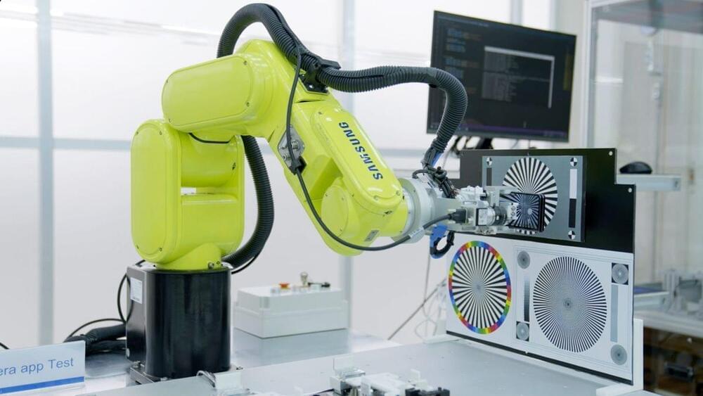
Knowing that current methods to detect viruses and other biological markers of disease are effective, yet large and expensive (such as fluorescence microscopes), a team of researchers at the University of Tokyo (Tokyo, Japan) has developed and tested a miniaturized virus-scanning system that makes use of low-cost components and a smartphone. The researchers hope the system could aid those who tackle the spread of diseases faster, as current tools—while highly accurate at counting viruses—are too cumbersome for many situations, especially when rapid diagnosis is required.

The newly developed device, which scans biological samples for real viruses, is portable, low-cost, and battery-powered. Yoshihiro Minagawa from the University of Tokyo, who led the development, tested the device with viruses, but says it could also detect other biological markers.

“I wanted to produce a useful tool for inaccessible or less-affluent communities that can help in the fight against diseases such as influenza,” says Minagawa. “Diagnosis is a critical factor of disease prevention. Our device paves the way for better access to essential diagnostic tools.”

A 3D-printed device in a tank of water braids nanowires and moves microparticles.

New antennae to access higher and higher frequency ranges will be needed for the next generation of phones and wireless devices. One way to make antennae that work at tens of gigahertz — the frequencies needed for 5G and higher devices — is to braid filaments about 1 micrometer in diameter. However, today’s industrial fabrication techniques won’t work on fibers that small.

“It was a shout-out-loud-in-joy moment when — on our first try — we crossed two fibers using only a piece of plastic, a water tank, and a stage that moves up and down.” —

The invention could enhance the speed of electronic devices and improve security screening technology.

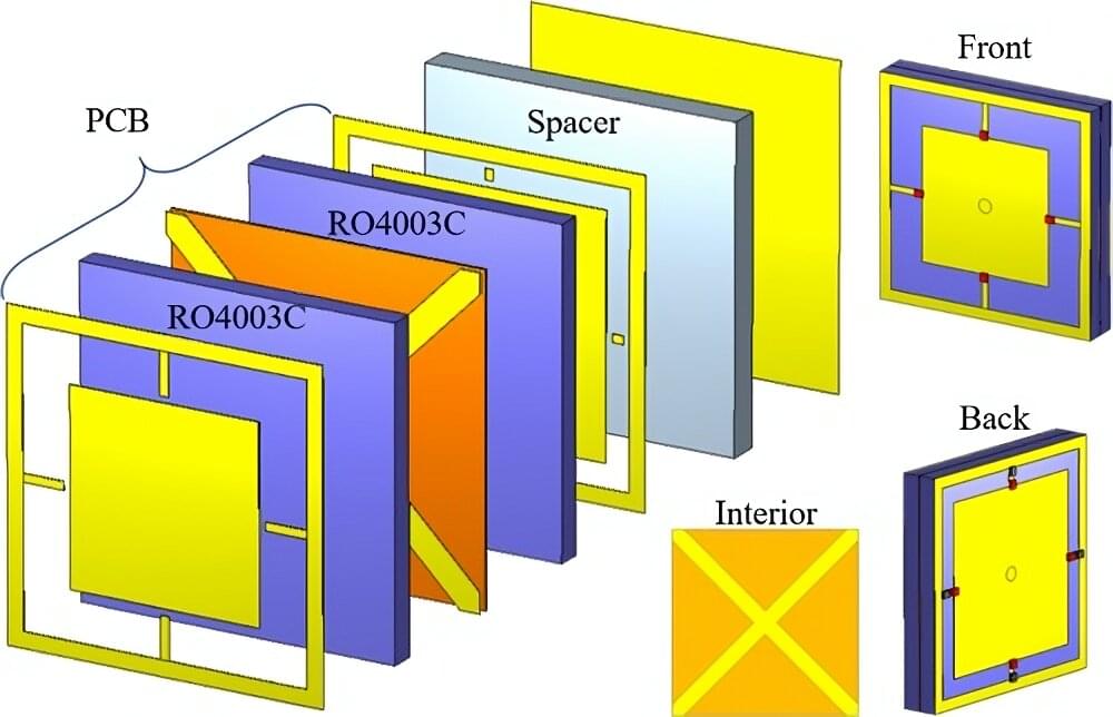
Chinese scientists have conceived of a new method for generating laser-like light that could significantly enhance the communication speed of everyday electronics, according to a report by the South China Morning Post.

The new device that makes this light possible is known as a free-electron laser, and it has been developed by scientists from the Shanghai Institute of Optics and Fine Mechanics under the Chinese Academy of Sciences.

The technology is not entirely new.


Memory and storage chip maker Micron Technology says it is shipping samples of the most bit-dense DRAM memory chips yet. Compared with its own previous generation, the 16-gigabit DRAM chip is 15 percent more power efficient and 35 percent more dense. Notably, Micron achieved the improvement without resorting to the most advanced chip-making technology, extreme ultraviolet lithography. The features that make up DRAM cells are not nearly as tiny as those on logic chips, but this advance shows that DRAM density could still shrink further in the future.

Micron says it is shipping samples of LPDDR5X chips, memory made for power-constrained systems such as smartphones. (LPDDR5X, unpacked: a revved-up twist on the low-power version of the fifth generation of the double-data-rate memory communications standard, capable of transferring 8.5 gigabits per second.) It’s the first chip made using Micron’s new manufacturing process, called 1-beta, which the company says maintains the lead it took a year ago over rivals, including Samsung and SK Hynix.

Manufacturing processes for DRAM and logic chips diverged decades ago, with logic chips shrinking transistors much more aggressively as the years went by, explains Jim Handy, a memory and storage analyst at Objective Analysis, in Los Gatos, Calif. The reason for the difference has to do with DRAM’s structure. DRAM stores a bit as charge in a capacitor. Access to each capacitor is gated by a transistor. But the transistor is an imperfect barrier, and the charge will eventually leak away. So DRAM must be periodically refreshed, restoring its bits before they drain away. In order to keep that refresh period reasonable while still increasing the density of memory, DRAM makers had to make some pretty radical changes to the makeup of the capacitor. For Micron and other major manufacturers, it now resembles a tall pillar and is made using materials not found in logic chips.

To produce the next generation of high-frequency antennae for 5G, 6G and other wireless devices, a team at the Harvard John A. Paulson School of Engineering and Applied Sciences (SEAS) has invented the machine and manufacturing technique to manipulate microscopic objects using 3D printing and braid them into filaments a mere micrometre in diameter.

How small is this? One human hair varies in diameter between 20 and 200 micrometres from tip to root. Spider web silk can vary from 3 to 8 micrometres in diameter. So that’s teeny tiny. And for us to pack in the many antennae that go into mobile phone technology today, the smaller the better.

Current manufacturing techniques can’t make one-micrometre filaments. But the machine invented by the Harvard SEAS team can. How does it do it? It uses the surface tension of water to grab and manipulate micromaterials. The capillary forces in the water are harnessed to help in the assembly using the variable width channels contained within the machine. Using 3D printing and the hydrophilic properties of the machine’s walls, the team used surface tension to guide kevlar nanowires attached to small floats which as they travelled through the device plaited into micrometre-scale braids.