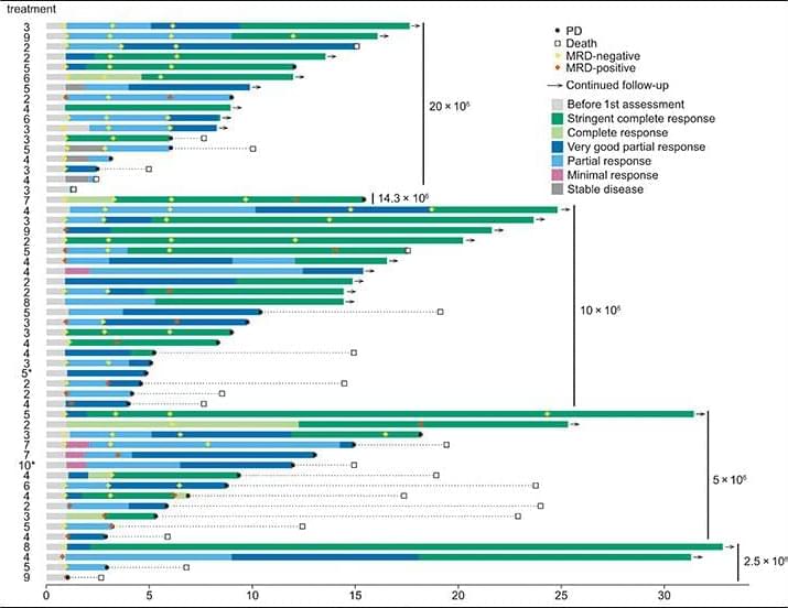
IN A NUTSHELL đ Chinaâs dominance in gallium production is reshaping global semiconductor and battery industries. â ïž Japan has raised alarms about the strategic implications of Chinaâs control over critical resources like gallium, germanium, and antimony. đ The U.S. sanctions against China have intensified competition for strategic raw materials, leading to trade tensions. đ The
Category: materials – Page 7
The UMass Amherst-led team is challenging the common belief that perfect fillers are the best choice for creating thermally conductive polymers.
In the pursuit of developing next-generation materials for modern devices, materials that are lightweight, flexible, and highly efficient at dissipating heat, a research team led by the University of Massachusetts Amherst has uncovered a surprising insight: imperfection has its upsides.
Published in Science Advances.
Free-electron lasers (FELs) have an electron problem: a âdarkâ current that can propagate with the electron beam, limiting the performance of the system. Now Guan Shu of Zhangjiang Laboratory in China and colleagues have developed a method that can reduce the strength of this unwanted dark current by 3 orders of magnitude [1]. Because their method requires no structural changes to existing equipment, Shu says it could be easily implemented in existing FELs. Their bright beams of x raysâgenerated by electronsâare increasingly popular for structural studies.
Most high-repetition-rate free-electron lasers are fed by very-high-frequency (VHF) electron guns. A VHF electron gun contains a photocathode that releases electrons when hit with a laser. These electrons are accelerated by a strong electric field and exit the photocathode as a beam through a port at the front. But the same field generates other electrons by pulling them off the photocathodeâs surface and from nearby copper surfaces via the field effect. These so-called dark electronsâthey donât need light to free themâcan cause unwanted heating that degrades the main electron beam and damages the beam line.
To weaken the dark current, researchers have typically lowered the gun voltage. But that route reduces the brightness of the main electron beam. Shu and colleagues found an alternative solution: modifying the plug upon which the photocathode material is deposited and grown. The team showed that by pushing the plug around 0.5â1 mm deeper than a standard plug, they were able to reduce the intensity of the dark current by nearly 2 orders of magnitude. The over-inserted plug also had another benefitâit defocused the dark current. Rather than propagating downstream to join the main beam, the dark current struck the VHF gun cavity walls before it could leave the photocathode.
An often-spouted complaint about public infrastructure projects is how long they take to complete. California High-Speed Rail, a perennial punching bag, is slated to get its initial operating segment running by 2031 at the earliest. A recent project in Japan flipped that notion on its head. The West Japan Railway Company, also known as JR West, replaced an entire station with 3D-printed prefabricated pieces in under three hours last week. The company also claims the construction costs were half that of reinforced concrete.
JR West used this new construction method to replace Hatsushima Station, a small wooden station built in 1949 and served less than 400 passengers per day. The company waited for an overnight lull in the schedule, then quickly sent its workers into action. The new station was pieced together with four hallow 3D-printed mortar pieces, according to the Japan Times. At the work site, the pieces were filled with rebar and concrete to provide the same earthquake resistance as traditionally built stations. Despite the blazing fast construction time, JR West aims to open the new station in July.
A new method called vdW squeezing enables the creation of stable, atomically thin 2D metals, opening doors to advanced devices and fundamental discoveries in materials science. Since the discovery of graphene in 2004, research into two-dimensional (2D) materials has advanced rapidly, opening new
Study found that magnetic order of chromium sulfide bromide can be turned on or offâlike a switchâby changing the temperature.
However, moderately significant changes have only been achieved under equilibrium conditions and at low temperatures. Significant differences at ambient temperatures, which are essential for applications, have so far been lacking.
For the first-ever time in collaboration with the theory groups of Angel Rubio (Max-Planck Institute, Hamburg) and Pascal Ruello (Université de Le Mans), EPFL scientists were able to control the excitonic properties using acoustic waves.
Scientists launched a high-frequency, large-amplitude acoustic wave in a material using ultrashort laser pulses. Doing this allowed them to manipulate the exciton properties at high speed. This astounding outcome was reached on titanium dioxide at room temperature, a cheap and abundant semiconductor that is used in a wide variety of light-energy conversion technologies, for example, photovoltaics, photocatalysis, and transparent conductive substrates.
A new on-chip sensor using twisted moirĂ© photonic crystals can precisely tune light properties in real time. This could replace bulky optical systems with one compact, powerful chip. Twisted moirĂ© photonic crystals â a cutting-edge type of optical metamaterial â hold significant promise for build
Two-dimensional (2D) semiconductor materials could enable the development of smaller yet highly performing electronic components, thus contributing to the advancement of a variety of devices. While significant strides have been made in the synthesis of 2D semiconductors with advanced electronic properties, their clean transfer onto substrates and reliable integration in real devices has so far proved challenging.
Researchers at Peking University, the Beijing Graphene Institute and other institutes in China have recently developed a new method to integrate 2D semiconductors with dielectric materials, which are insulating materials that help control the flow of electric charge in devices. Their approach, outlined in a paper published in Nature Electronics, entails the epitaxial growth of an ultra-thin dielectric film on a graphene-covered copper surface, which subsequently enables its transfer onto various substrates with minimal defects.
âThe paper emerged from recognizing persistent challenges in integrating two-dimensional materialsâsuch as grapheneâinto microelectronic devices,â Zhongfan Liu, Li Lin, and Yanfeng Zhang, corresponding authors of the paper, told Tech Xplore.
Fluids play a crucial role in industrial processes like cooling, heating, and mixing. Traditionally, most industries would utilize Newtonian fluidsâwhich have a constant viscosityâfor such processes. However, many are now adopting viscoelastic fluids, which can behave as both liquids and elastic materials.
These fluids can suppress turbulence in simple flows like straight pipes or channels, leading to reduced wall friction. This âdrag reduction effectâ has attracted significant interest due to its potential to enhance energy efficiency.
To advance the industrial applications of such fluids, it is critical to understand how these fluids interact with turbulence.