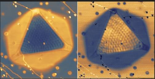
An atomic single electron transistor, which utilizes a single atomic defect in a van der Waals material as an ultrasensitive, high-resolution potential sensor, is used to image the electrostatic potential within a moiré unit cell.
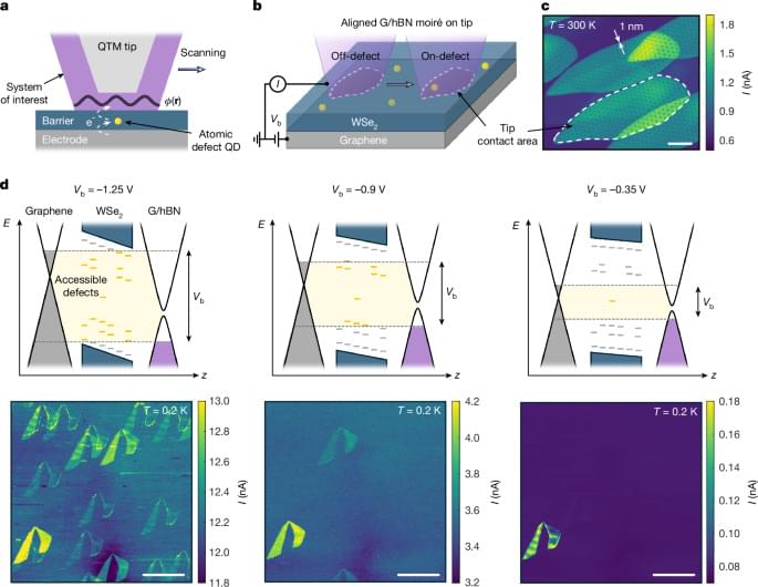

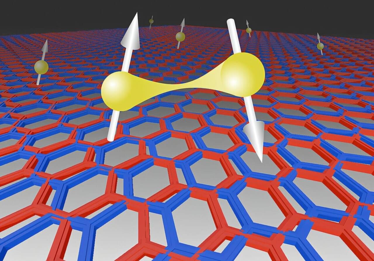
How exactly unconventional superconductivity arises is one of the central questions of modern solid-state physics. A new study published in the journal Nature provides crucial insights into this question. For the first time, an international research team was able to demonstrate a direct microscopic connection between a strongly correlated normal state and superconductivity in so-called moiré materials. In the long term, these findings could contribute to the development of new quantum materials and superconductors for future quantum technologies.
Professor Giorgio Sangiovanni from the Institute of Theoretical Physics and Astrophysics at Julius-Maximilians-Universität Würzburg (JMU) was involved in the study. His research is part of the Cluster of Excellence ctd.qmat—Complexity, Topology and Dynamics in Quantum Matter—at JMU and the Technical University of Dresden.
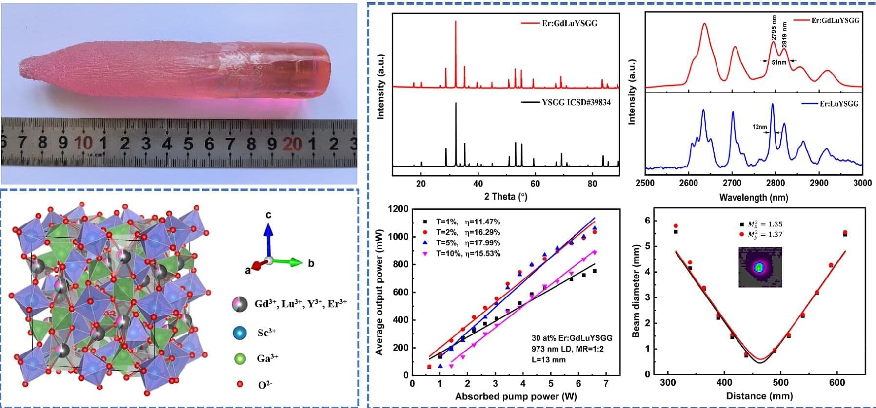
Recently, a research team from the Hefei Institutes of Physical Science of the Chinese Academy of Sciences successfully grew a high-entropy garnet-structured oxide crystal and achieved enhanced laser performance at the 2.8 μm wavelength band. By introducing a high-entropy design into a garnet crystal system, the team obtained a wide emission band near 2.8 μm and continuous-wave laser output with improved average power and beam quality, demonstrating the material’s strong potential as a high-performance gain medium for mid-infrared ultrashort-pulse lasers.
The results are published in Crystal Growth & Design.
Mid-infrared ultrashort-pulse lasers around 2.8 μm are of great interest for applications such as space communication and planetary exploration. However, existing laser crystals operating in this wavelength range often suffer from narrow emission bandwidths, low efficiency, or insufficient radiation resistance, making it difficult to meet the demands of efficient and stable laser operation in harsh space radiation environments.
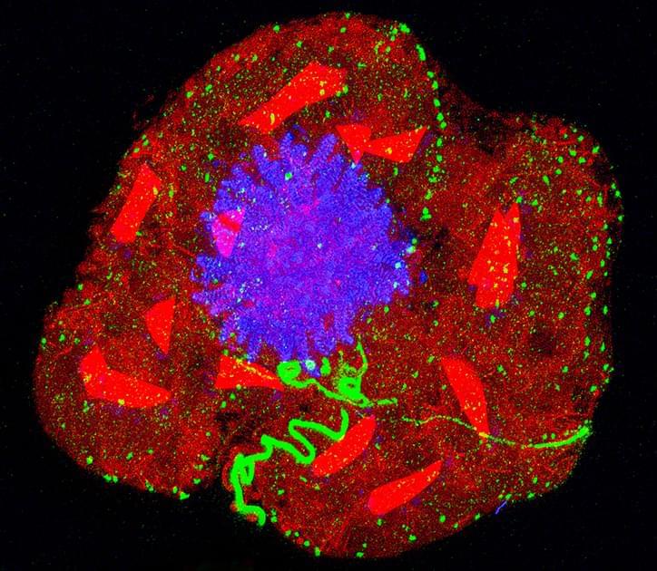
Expansion microscopy is possible for any lab with a basic microscope. Specific biomolecules such as proteins are anchored to a hydrogel. As the gel absorbs added water, it swells and the space between the anchor points dilates. This allows researchers to visualize extra-tiny anatomy or see inside cells with tough barriers.
How physically magnifying objects using a key ingredient in diapers has opened an unprecedented view of the microbial world.
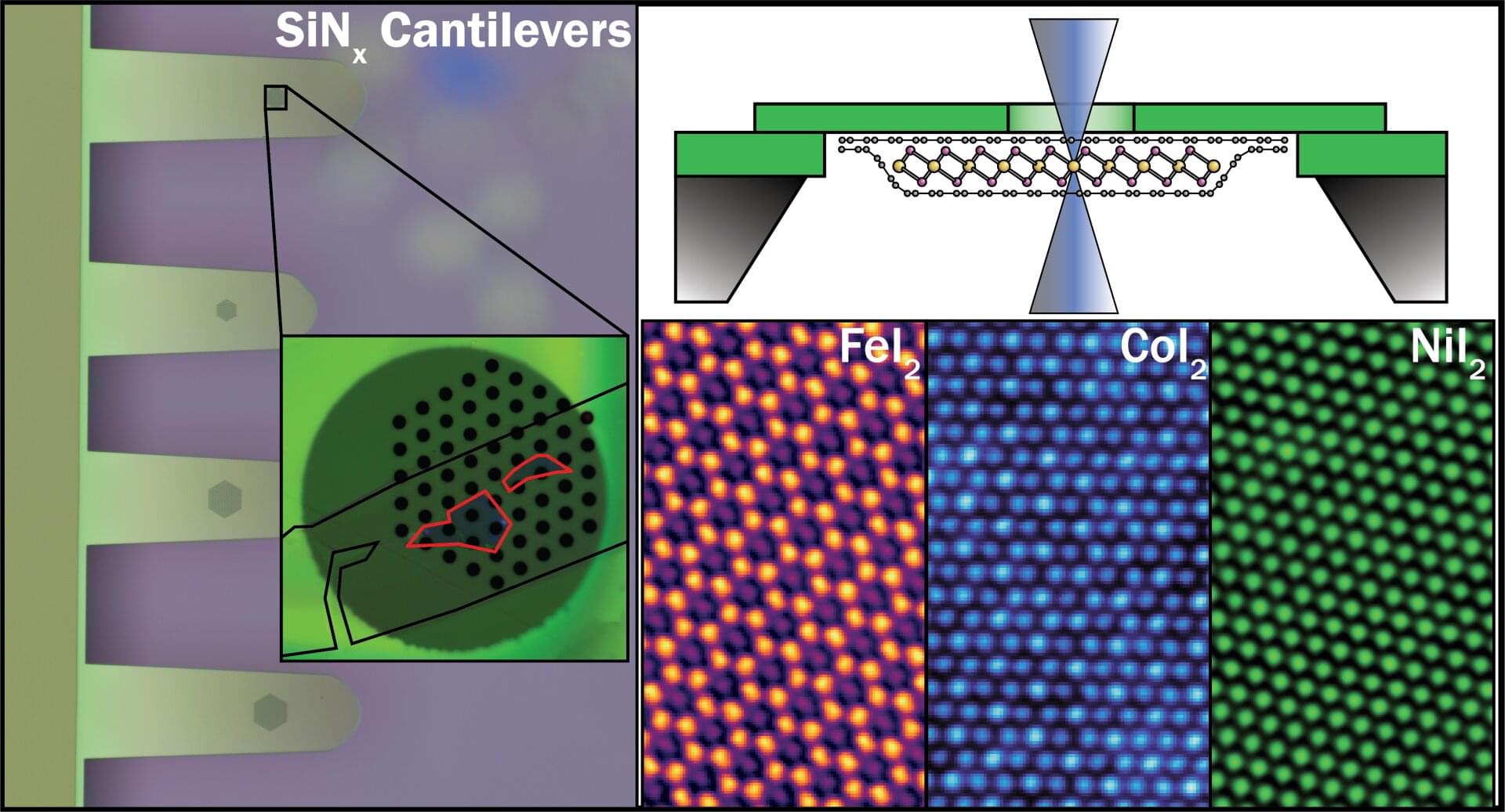
Two-dimensional (2D) materials promise revolutionary advances in electronics and photonics, but many of the most interesting candidates degrade within seconds of air exposure, making them nearly impossible to study or integrate into real-world technology. Transition metal dihalides represent a particularly compelling yet challenging class of materials, with predicted properties ideal for next-generation devices, but their extreme reactivity when exposed to air prevents even basic structural characterization.
Researchers at The University of Manchester’s National Graphene Institute have now achieved the first atomic-resolution imaging of monolayer transition metal diiodides, made possible by creating graphene-sealed TEM samples that prevent these highly reactive materials from degrading on contact with air.
The study, published in ACS Nano, demonstrates that fully encapsulating the crystals in graphene preserves atomically clean interfaces and extends their usable lifetime from seconds to months.

Physicists have uncovered surprising order inside one of the most puzzling states in modern materials science. It is a strange middle ground where electrons begin to behave differently, but full superconductivity has not yet taken hold.
Instead of falling into disorder, the system retains coordinated patterns right at the point where normal electrical behavior starts to break down. The finding suggests this transition is guided by an underlying structure, not randomness.
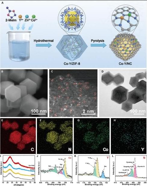
JUST PUBLISHED: JUST PUBLISHED: d–d/p Orbital Hybridization in Symmetry-Broken Co–Y Diatomic Sites Enables Efficient Na–S Battery.
Read the latest free, Open Access article from Energy Material Advances.
Despite advances of single-atom catalysts (SACs) in sodium–sulfur (Na–S) batteries, their symmetric coordination geometry (e.g., M–N4) fundamentally restricts orbital-level modulation of sulfur redox kinetics. Herein, we demonstrate that hetero-diatomic Co–Y sites with Co–N4–Y–N4 coordination on N-doped carbon (Co–Y/NC) break the M–N4 symmetry constraint through d–d orbital hybridization, which is confirmed by an implementation of advanced characterizations, including the high-angle annular dark-field scanning transmission electron microscopy and x-ray absorption fine structure spectroscopy. In practical operation, the Co–Y/NC@S cathode with 61% sulfur mass fraction delivers a superior capacity (1,109 mAh/g) at 0.2 A/g, outperforming that of Co or Y SAC and further setting a new benchmark of diatomic catalysts for Na–S battery systems.
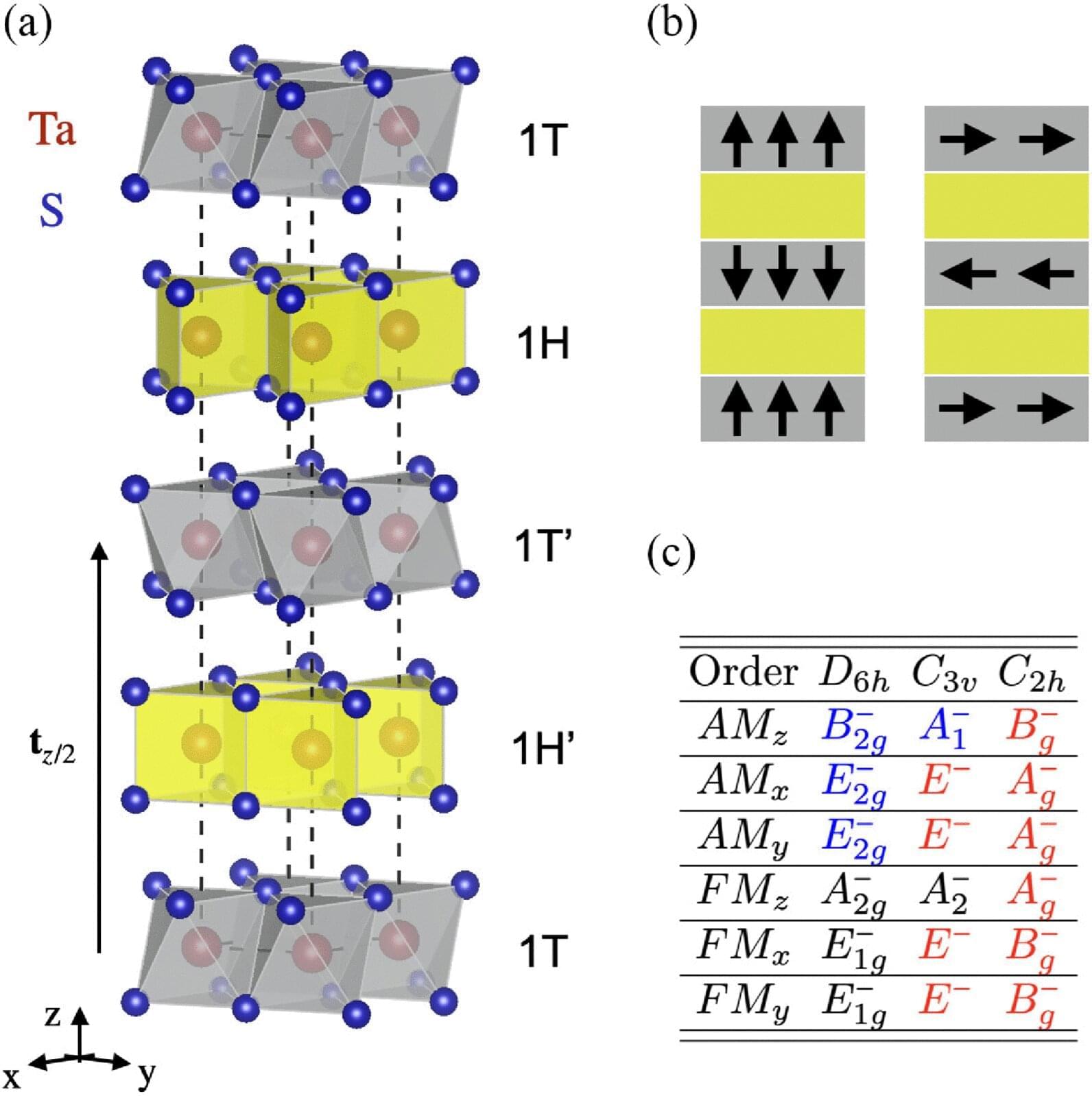
How are superconductivity and magnetism connected? A puzzling relation between magnetism and superconductivity in a quantum material has lingered for decades—now, a study from TU Wien offers a surprising new explanation.
Some materials conduct electricity without any resistance when cooled to very low temperatures. This phenomenon, known as superconductivity, is closely linked to other important material properties. However, as new work by physicist Aline Ramires from the Institute of Solid State Physics at TU Wien now shows: in certain materials, superconductivity does not generate exotic magnetic properties, as was widely assumed. Instead, it merely makes an unusual form of magnetism experimentally observable—so-called altermagnetism.