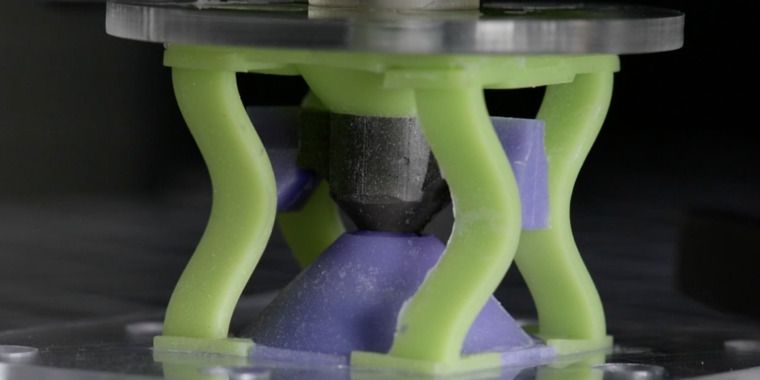
University of Texas at Arlington researchers have developed a technique that programs 2-D materials to transform into complex 3D shapes.


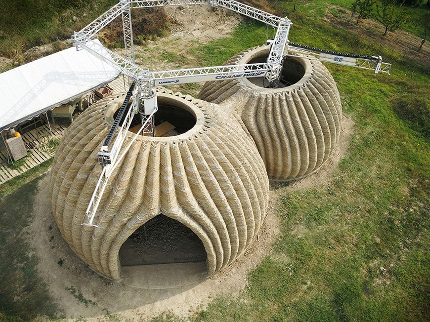
“TECLA (an acronym which stands for “Technology and Clay”) is a habitat consisting of two interconnected housing units, each covered by a semi-spherical dome. The units have been built using multiple Crane Wasp printing units operating simultaneously. Crane WASP is defined by the manufacturer as “a collaborative 3D printing system capable of printing houses” and can print various materials — such as earth-based materials, concrete mortar, and geopolymers — with a maximum speed of 300 mm/s and a maximum printing area of 50 sqm per unit. The design of the habitat features two or more “cocoon-like” housing units, whose shape vaguely resembles that of a sea urchin, in which structure, insulation, and finishes coincide. The thick raw earth walls of the units have a hollow structure consisting of several clay “waves”, which makes them at the same time relatively lightweight, resistant, and highly insulating. About 200 printing hours are required to build each unit, which consists of 350 clay layers, each 12 mm thick.”
Designed by Mario Cucinella and build by WASP, TECLA is a prototype house near Ravenna, Italy, made by 3D-printing a material based on locally-sourced clay.

3D printing is a universal process in the sense that pretty much any part that can be drawn up in a CAD program can be printed, at least within a certain resolution. Machining a part on a mill or lathe, while having the advantage of greater accuracy and material options, is a slightly less universal process in that many possible designs that exist in theory could never be machined. A hollow sphere can easily be printed, but a ball could never be milled as a single part into a hollow sphere—unless you happen to have a milling machine tiny enough to fit inside the ball. But what about biological parts, and whole animals? How universal, from a design perspective, is growth?

It was invented by David Gathu and Moses Kinyua and is powered by brain signals.
The signals are converted into an electric current by a “NeuroNode” biopotential headset receiver. This electrical current is then driven into the robot’s circuitry, which gives the arm its mobility.
The arm has several component materials including recycled wood and moves vertically and horizontally.
Juniorr Amenra.
· —3—h ·

I don’t think that star is the same after that one night stand.
When black holes swallow down massive amounts of matter from the space around them, they’re not exactly subtle about it. They belch out tremendous flares of X-rays, generated by the material heating to intense temperatures as it’s sucked towards the black hole, so bright we can detect them from Earth.
This is normal black hole behaviour. What isn’t normal is for those X-ray flares to spew forth with clockwork regularity, a puzzling behaviour reported in 2019 from a supermassive black hole at the centre of a galaxy 250 million light-years away. Every nine hours, boom — X-ray flare.
After careful study, astronomer Andrew King of the University of Leicester in the UK identified a potential cause — a dead star that’s endured its brush with a black hole, trapped on a nine-hour, elliptical orbit around it. Every close pass, or periastron, the black hole slurps up more of the star’s material.

Researchers at[ MIT have developed a new method for growing plant tissues in a lab](https://news.mit.edu/2021/lab-grown-plant-tissue-0120) — sort of like how companies and researchers are approaching lab-grown meat. The process would be able to produce wood and fibre in a lab environment, and researchers have already demonstrated how it works in concept by growing simple structures using cells harvested from zinnia leaves.
Researchers at MIT have developed a new method for growing plant tissues in a lab — sort of like how companies and researchers are approaching lab-grown meat. The process would be able to produce wood and fibre in a lab environment, and researchers have already demonstrated how it works in concept by growing simple structures using cells harvested from zinnia leaves.
This work is still in its very early stages, but the potential applications of lab-grown plant material are significant, and include possibilities in both agriculture and in construction materials. While traditional agricultural is much less ecologically damaging when compared to animal farming, it can still have a significant impact and cost, and it takes a lot of resources to maintain. Not to mention that even small environmental changes can have a significant effect on crop yield.
Forestry, meanwhile, has much more obvious negative environmental impacts. If the work of these researchers can eventually be used to create a way to produce lab-grown wood for use in construction and fabrication in a way that’s scalable and efficient, then there’s tremendous potential in terms of reducing the impact on forestry globally. Eventually, the team even theorizes you could coax the growth of plant-based materials into specific target shapes, so you could also do some of the manufacturing in the lab, by growing a wood table directly for instance.

A new discovery in the mountains of northern Israel has caused significant excitement for geologists around the world. While working in the Zevulun Valley, close to Mount Carmel, Israeli mining company Shefa Yamim found a new mineral never before discovered on earth.
The International Mineralogical Association regularly approves new minerals for its official list, with up to 100 new substances added to the register each year.
However, this latest discovery was hailed as a significant event, as it was previously believed that this type of mineral was only found on extraterrestrial material.

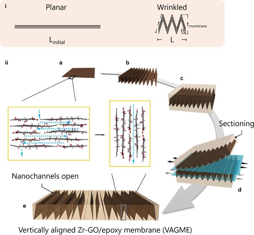
When sheets of two-dimensional nanomaterials like graphene are stacked on top of each other, tiny gaps form between the sheets that have a wide variety of potential uses. In research published in the journal Nature Communications, a team of Brown University researchers has found a way to orient those gaps, called nanochannels, in a way that makes them more useful for filtering water and other liquids of nanoscale contaminants.
“In the last decade, a whole field has sprung up to study these spaces that form between 2-D nanomaterials,” said Robert Hurt, a professor in Brown’s School of Engineering and coauthor of the research. “You can grow things in there, you can store things in there, and there’s this emerging field of nanofluidics where you’re using those channels to filter out some molecules while letting others go through.”
There’s a problem, however, with using these nanochannels for filtration, and it has to do with the way those channels are oriented. Like a notebook made from stacked sheets of paper, graphene stacks are thin in the vertical direction compared to their horizontal length and width. That means that the channels between the sheets are likewise oriented horizontally. That’s not ideal for filtration, because liquid has to travel a relatively long way to get from one end of a channel to the other. It would be better if the channels were perpendicular to the orientation of the sheets. In that case, liquid would only need to traverse the relatively thin vertical height of the stack rather than the much longer length and width.
