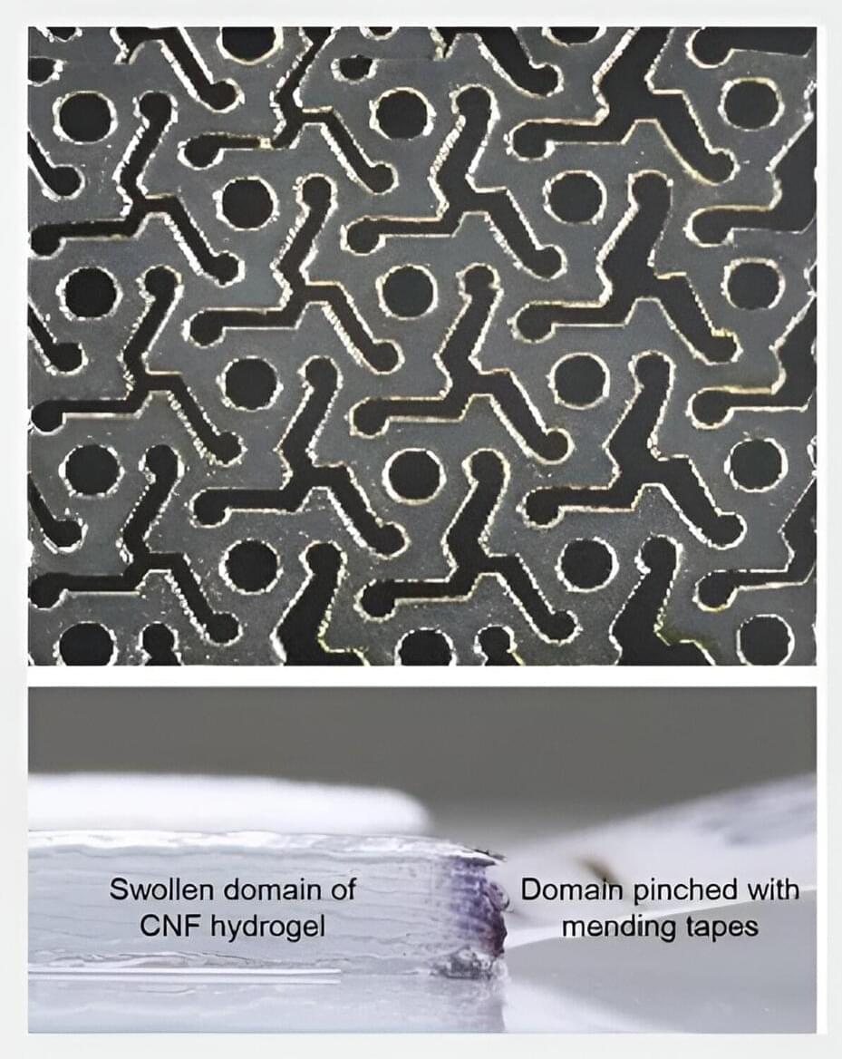
MIT researchers can now control the physical and mechanical properties of lab-grown plant materials. This could enable an environmentally friendly process to produce wood-like structures with specific properties, like stiffness or density, tailored to certain applications.
Archive for the ‘materials’ category: Page 146
May 25, 2022
Your Martian Dream Home, Made By Fungi
Posted by Jose Ruben Rodriguez Fuentes in categories: materials, space
Your Martian Dream Home, Made By Fungi ‘… it was the cheapest building material known.’ — Larry Niven, 1968.
3D Printed Glass Uses Stereolithography Techniques ‘All that with glass…’ — Frank Herbert, 1972.
Circa 1978
Summary. The energetics of the gravitationally powered dynamo have been studied with the aid of a compressible-earth model which allows for the growth of the solid inner core. The basic premise of this study is that as the Earth gradually cooled over geological time the solid inner core continually accreted dense material which crystallized from an outer core composed of a molten binary alloy. This process requires a continual rearrangement of matter which generates the fluid motions needed to sustain the dynamo. These motions maintain the outer core in a well-mixed state, in apparent contradiction to Higgins & Kennedy’s hypothesis that the outer core is stably stratified. The vigour of these motions is dependent primarily upon the composition of the solid inner core, but is surprisingly independent of the density of the light constituent in the core. If the solid core is composed entirely of heavy metal, then as much as 3.7 × 10¹² W may be transferred from the core to the mantle as a result of cooling and gravitational settling. This is roughly equal to estimates of the amount of heat conducted down the adiabat in the core, but it is argued that there is no direct relation between the amount of heat conducted down the adiabat and the amount transferred to the mantle if the convection is driven non-thermally. The gravitational energy released per unit mass of the solid inner core is remarkably constant and may be as much as 2 × 10⁶J/kg, roughly five times the value of the latent heat of iron. These values are reduced if the solid inner core contains some light constituents. It was found that the efficiency of the gravitationally powered dynamo may exceed 50 per cent, a much higher figure than is possible for either the thermally or precessionally driven dynamo. Also, the amount of gravitational energy available to drive the dynamo in the future is many times that expended so far. The size of the magnetic field sustained by gravitational settling was related to the density jump at the inner—outer core boundary and the field strength was estimated to lie between 390 and 685 G, strongly suggesting that the dynamo is of the nearly-axisymmetric type developed by Braginsky.
May 24, 2022
Metamaterials Control the Shape of Water Waves
Posted by Saúl Morales Rodriguéz in categories: materials, physics
A water wave incident on a grooved wall is shown to be analogous to electromagnetic waves called surface plasmon polaritons.
The ability of metamaterials to steer light has enabled amazing inventions from superresolution microscopes to “invisiblity” cloaks. But the physics underlying these structures also applies to other waves, such as acoustic, seismic, and water waves. Huanyang Chen and his colleagues at Xiamen University in China have demonstrated a structure that can change the propagation of surface water waves, making a localized wave that is analogous to an electromagnetic excitation called a surface plasmon polariton [1].
Surface plasmon polaritons occur at the interface between a dielectric and a negative-permittivity material such as a metal. Generating an equivalent excitation in surface water waves requires a similar sort of interface, such as that between water and a vertical barrier. In this case, the water’s parameter that is analogous to a metal’s permittivity is its depth. Of course, it’s impossible for water to have negative depth, but using metamaterials, Chen and his colleagues engineered the boundary conditions of the waves to achieve the same effect.
May 23, 2022
Topological Materials Are Everywhere — New Database Reveals Over 90,000
Posted by Jose Ruben Rodriguez Fuentes in categories: materials, mathematics
Searchable tool reveals more than 90,000 known materials with electronic properties that remain unperturbed in the face of disruption.
What will it take for our electronics to become smarter, faster, and more resilient? One idea is to build them out of topological materials.
Topology stems from a branch of mathematics that studies shapes that can be manipulated or deformed without losing certain essential properties. A donut is a common example: If it were made of rubber, a donut could be twisted and squeezed into a completely new shape, such as a coffee mug, while retaining a key trait — namely, its center hole, which takes the form of the cup’s handle. The hole, in this case, is a topological trait, robust against certain deformations.
May 23, 2022
Paper-based semiconductor aids the drive for sustainable electronics
Posted by Jose Ruben Rodriguez Fuentes in categories: materials, sustainability
According to the team, the new semiconducting cellulose nanopaper (CNP) can be tailored for a variety of applications. The paper itself can be shaped into different designs and the material’s electrical conduction properties can be tuned from 1012 to 10–2 Ω cm – values that exceed those of previously-reported 3D semiconducting materials – by changing the concentration of charge carriers (electrons and holes) in it. This means it is suitable for use in many devices, from water vapour sensors to electrodes in enzymatic biofuel cells.
May 23, 2022
Can you reinvent the wheel? Scientists synthesized a new kind of graphene
Posted by Gemechu Taye in category: materials
May 23, 2022
New electronics cooling tech enables 740% increase in power per unit volume
Posted by Shubham Ghosh Roy in categories: engineering, materials
Tarek Gebrael, a UIUC Ph.D. student in mechanical engineering, explains that the existing solutions suffer from three shortcomings – first, they can be expensive and difficult to scale up. Second, conventional heat spreading approaches generally require that the heat spreader and a heat sink be attached on top of the electronics device. Unfortunately, in many cases, most of the heat is generated underneath the electronic devices, meaning that the cooling mechanism isn’t where it is needed the most.
And third, Gebrael explained, the heat spreaders can’t be installed directly on the surface of the electronics. They require a layer of “thermal interface material” sandwiched between them to ensure good contact. However, due to its poor heat transfer characteristics, that middle layer also introduces a negative impact on thermal performance.
Now, researchers have come up with a new solution to address all three of those problems. First, they used copper as a primary material, which is relatively inexpensive. They then made the copper coating that entirely “engulfs” the device, says Gebrael, “covering the top, the bottom, and the sides… a conformal coating that covers all the exposed surfaces” – so that no heat-producing regions are neglected. And finally, the new solution removes the need for a thermal interface material and a heat sink.
May 22, 2022
Imec Presents Sub-1nm Process and Transistor Roadmap Until 2036: From Nanometers to the Angstrom Era
Posted by Jamal Simpson in categories: computing, materials
Imec plots a course to 1nm chips, and beyond.
Imec, the most advanced semiconductor research firm in the world, recently shared its sub-‘1nm’ silicon and transistor roadmap at its Future Summit event in Antwerp, Belgium. The roadmap gives us a rough idea of the timelines through 2036 for the next major process nodes and transistor architectures the company will research and develop in its labs in cooperation with industry giants, like TSMC, Intel, Samsung, and ASML, among many others.
The roadmap includes breakthrough transistor designs that evolve from the standard FinFET transistors that will last until 3nm, to new Gate All Around (GAA) nanosheets and forksheet designs at 2nm and A7 (seven angstroms), respectively, followed by breakthrough designs like CFETs and atomic channels at A5 and A2. As a reminder, ten Angstroms are equal to 1nm, so Imec’s roadmap encompasses sub-‘1nm’ process nodes.
May 19, 2022
Spin keeps electrons in line in iron-based superconductor
Posted by Shubham Ghosh Roy in categories: materials, quantum physics
Researchers from PSI’s Spectroscopy of Quantum Materials group together with scientists from Beijing Normal University have solved a puzzle at the forefront of research into iron-based superconductors: the origin of FeSe’s electronic nematicity. Using Resonant inelastic X-ray scattering (RIXS) at the Swiss Light Source (SLS), they discovered that, surprisingly, this electronic phenomenon is primarily spin driven.
Electronic nematicity is believed to be an important ingredient in high-temperature superconductivity, but whether it helps or hinders it is still unknown.
Their findings are published in Nature Physics (“Spin-excitation anisotropy in the nematic state of detwinned FeSe”).