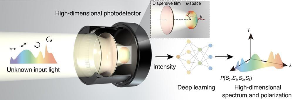
Our photodetector is capable of demonstrating high spectral resolution and accurate reconstruction of full-Stokes polarization states in both theoretical and experimental settings. Precision detection of high-dimensional information by our photodetector, such as a two-color laser field with different polarization states or broadband reflection from a gold interface exhibiting varying polarization states, is achieved beyond the capabilities of commercial polarimeter and spectrometer.
Additionally, this approach can be extended to imaging applications by sandwiching the film with a commercial microlens array and sensor array to realize ultra-compact high-dimensional imager, said Assistant Professor Chunqi Jin from the Changchun Institute of Optics, Fine Mechanics and Physics (CIOMP) of the Chinese Academy of Sciences.
Looking ahead, Prof. Wei Li envisions that ultra-broadband detection can be achieved by integrating broadband commercial photodetectors; the detection resolution can be further improved by using photonic crystals, metasurfaces, and two-dimensional materials instead of existing thin film schemes; and the detection capability can be stepped up in higher dimensions by integrating functionalities such as image processing, and distance measurement.


