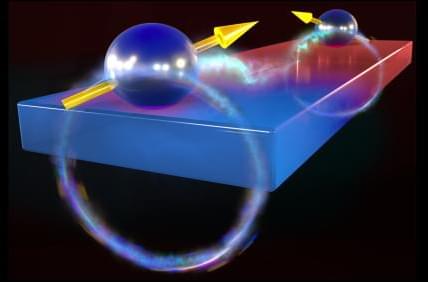
Toggle light / dark theme

Researchers have reported the discovery of an exoplanet orbiting Ross 508 near the inner edge of its habitable zone.


Researchers at the University of Massachusetts Amherst recently announced that they have figured out how to engineer a biofilm that harvests the energy in evaporation and converts it to electricity. This biofilm, which was announced in Nature Communications, has the potential to revolutionize the world of wearable electronics, powering everything from personal medical sensors to personal electronics.

“This is a very exciting technology,” says Xiaomeng Liu, graduate student in electrical and computer engineering in UMass Amherst’s College of Engineering and the paper’s lead author. “It is real green energy, and unlike other so-called ‘green-energy’ sources, its production is totally green.”

That’s because this —a thin sheet of bacterial cells about the thickness of a sheet of paper—is produced naturally by an engineered version of the bacteria Geobacter sulfurreducens. G. sulfurreducens is known to produce electricity and has been used previously in “microbial batteries” to . But such batteries require that G. sulfurreducens is properly cared for and fed a constant diet. By contrast, this new biofilm, which can supply as much, if not more, energy than a comparably sized battery, works, and works continuously, because it is dead. And because it’s dead, it doesn’t need to be fed.

Scientists at the Lawrence Livermore National Laboratory (LLNL) Energetic Materials Center and Purdue University Materials Engineering Department have used simulations performed on the LLNL supercomputer Quartz to uncover a general mechanism that accelerates chemistry in detonating explosives critical to managing the nation’s nuclear stockpile. Their research is featured in the July 15 issue of the Journal of Physical Chemistry Letters.

Insensitive high explosives based on TATB (1,3,5-triamino-2,4,6-trinitrobenzene) offer enhanced safety properties over more conventional explosives, but physical explanations for these safety characteristics are not clear. Explosive initiation is understood to arise from hotspots that are formed when a shockwave interacts with microstructural defects such as pores. Ultrafast compression of pores leads to an intense localized spike in temperature, which accelerates chemical reactions needed to initiate burning and ultimately . Engineering models for insensitive high explosives—used to assess safety and performance—are based on the hotspot concept but have difficulty in describing a wide range of conditions, indicating missing physics in those models.

Using large-scale atomically resolved reactive molecular dynamics supercomputer simulations, the team aimed to directly compute how hotspots form and grow to better understand what causes them to react.

The startup is hiring Ritesh Jain, VP of engineering at Intel, to help it move from the prototype phase of its chip development to mass production.


ESA is prepping to send a spacecraft to Venus — a feat which will require state-of-the-art methods to get through the planet’s grueling atmosphere.

The subtractive manufacturing process involves etching, drilling, or cutting from a solid board to build the final product. It is ideal for applications using a wide variety of materials and in the PCB fabrication of large-size products. In the additive manufacturing process, a product is developed by adding material one layer at a time and bonding the layers together until the final product is ready. The ability to control material density and the possibility of including intricate features makes this process versatile. It is used in a range of engineering and manufacturing applications, especially in custom manufacturing.

Benefits of 3D printing in medical device manufacturing.

3D printing is economical and offers quick PCB prototyping without the need for complex manufacturing steps. It optimizes the PCB design process by avoiding possible design faults in the initial PCB design stages. 3D printing is easy on flex PCBs and multilayer PCB printing is possible using the latest design software. With the growing manufacturing trends and improving software, 3D printing will be more than a prototyping tool and can be a viable alternative for production parts. 3D printing has been recently used for the end-part manufacturing of several medical devices like hearing aids, dental implants, and more. It is more beneficial for low-volume productions.

Circa 2013 😃


News: the world’s first building to be powered entirely by algae is being piloted in Hamburg, Germany, by engineering firm Arup.

The “bio-adaptive facade”, which Arup says is the first of its kind, uses live microalgae growing in glass louvres to generate renewable energy and provide shade at the same time.

Installed in the BIQ building as part of the International Building Exhibition, the algae are continuously supplied with liquid nutrients and carbon dioxide via a water circuit running through the facade.

Quantum entanglement is one of the most fundamental and intriguing phenomena in nature. Recent research on entanglement has proven to be a valuable resource for quantum communication and information processing. Now, scientists from Japan have discovered a stable quantum entangled state of two protons on a silicon surface, opening doors to an organic union of classical and quantum computing platforms and potentially strengthening the future of quantum technology.

One of the most interesting phenomena in quantum mechanics is “quantum entanglement.” This phenomenon describes how certain particles are inextricably linked, such that their states can only be described with reference to each other. This particle interaction also forms the basis of quantum computing. And this is why, in recent years, physicists have looked for techniques to generate entanglement. However, these techniques confront a number of engineering hurdles, including limitations in creating large number of “qubits” (quantum bits, the basic unit of quantum information), the need to maintain extremely low temperatures (1 K), and the use of ultrapure materials. Surfaces or interfaces are crucial in the formation of quantum entanglement. Unfortunately, electrons confined to surfaces are prone to “decoherence,” a condition in which there is no defined phase relationship between the two distinct states.

A novel bioremediation technology for cleaning up per-and polyfluoroalkyl substances, or PFAS, chemical pollutants that threaten human health and ecosystem sustainability, has been developed by Texas A&M AgriLife researchers. The material has potential for commercial application for disposing of PFAS, also known as “forever chemicals.”

Published July 28 in Nature Communications, the was a collaboration of Susie Dai, Ph.D., associate professor in the Texas A&M Department of Plant Pathology and Microbiology, and Joshua Yuan, Ph.D., chair and professor in Washington University in St. Louis Department of Energy, Environmental and Chemical Engineering, formerly with the Texas A&M Department of Plant Pathology and Microbiology.

Removing PFAS contamination is a challenge

PFAS are used in many applications such as food wrappers and packaging, dental floss, fire-fighting foam, nonstick cookware, textiles and electronics. These days, PFAS are widely distributed in the environment from manufacturing or from products containing the chemicals, said Dai.

A team of researchers from the National University of Singapore (NUS) has developed a novel technique that allows Physically Unclonable Functions (PUFs) to produce more secure, unique ‘fingerprint’ outputs at a very low cost. This achievement enhances the level of hardware security even in low-end systems on chips.

Traditionally, PUFs are embedded in several commercial chips to uniquely distinguish one from another by generating a secret key, similar to an individual fingerprint. Such a technology prevents hardware piracy, chip counterfeiting and physical attacks.

The research team from the Department of Electrical and Computer Engineering at the NUS Faculty of Engineering has taken silicon chip fingerprinting to the next level with two significant improvements: firstly, making PUFs self-healing; and secondly, enabling them to self-conceal.

Perovskite solar cells (PSCs) are promising solar technologies. Although low-cost wet processing has shown advantages in small-area PSC fabrication, the preparation of uniform charge transport layers with thickness of several nanometers from solution for meter-sized large area products is still challenging.

Recently, a research group led by Prof. LIU Shengzhong from the Dalian Institute of Chemical Physics (DICP) of the Chinese Academy of Sciences (CAS) has developed a facile surface redox engineering (SRE) strategy for vacuum-deposited NiO x to match the slot-die-coated perovskite, and fabricated high-performance large-area perovskite submodules.

This work was published in Joule (“Surface redox engineering of vacuum-deposited NiO x for top-performance perovskite solar cells and modules”).