Francis Halzen, the lead scientist of the IceCube Neutrino Detector, explains how light sensors buried deep in the ice at the South Pole detected a neutrino that traveled four billion light-years.


Francis Halzen, the lead scientist of the IceCube Neutrino Detector, explains how light sensors buried deep in the ice at the South Pole detected a neutrino that traveled four billion light-years.

Of all the science-fiction-sounding names that have come to fruition in recent years, perhaps none is as mysterious or seemingly fictitious as time crystals. The name evokes something between Back to the Future and Donnie Darko, and the reality is perhaps crazier than either.
Two separate groups of scientists recently reported that they observed time crystals, which lends credence to the idea that this theoretical state of matter is something humans can actually create and observe. And indeed, time crystals can be grown in a child’s bedroom.
However, it requires nuclear sensors and lasers to help time crystals reach their full potential and then measure and observe them. This combination of dramatic scientific terms and shockingly simple objects is a great analogy for time crystals as a whole.
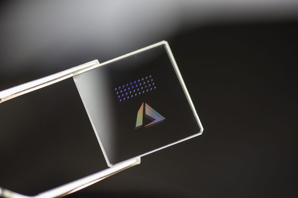
Is developing the first-ever storage technology designed and built from the media up, for the cloud. We are leveraging recent discoveries in ultrafast laser optics to store data in quartz glass by using femtosecond lasers, and building a completely new storage system designed from scratch around this technology. This opens up an incredibly exciting opportunity to challenge and completely re-think traditional storage system design, and to co-design the future hardware and software infrastructure for the cloud.
We are hiring for this and related projects: Post-Doc Researchers in Storage Software and Optical Systems, and internships in Software, FPGA, Electronics and Optics.
This project is a collaboration with the University of Southampton Optoelectonics Research Centre, and was featured in a Microsoft Ignite 2017 keynote on future storage technologies.
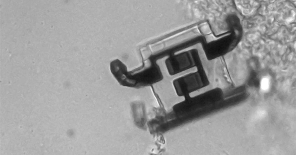
Some 70% of Earth’s surface is covered by water, and yet nearly all earthquake detectors are on land. Aside from some expensive battery-powered sensors dropped to the sea floor and later retrieved, and a few arrays of near-shore detectors connected to land, seismologists have no way of monitoring the quakes that ripple through the sea floor and sometimes create tsunamis. Now, a technique described online in Science this week promises to take advantage of more than 1 million kilometers of fiber optic cables that crisscross the ocean floors and carry the world’s internet and telecom traffic. By looking for tiny changes in an optical signal running along the cable, scientists can detect and potentially locate earthquakes. The technique requires little more than lasers at each end of the cable and access to a small portion of the cable’s bandwidth. Crucially, it requires no modification to the cable itself and does not interfere with its everyday use.


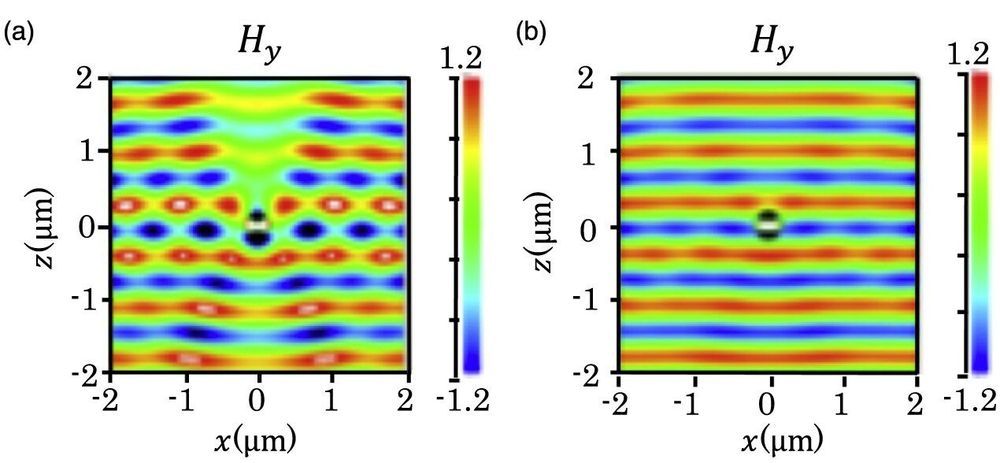
A pair of researchers at Tokyo Institute of Technology (Tokyo Tech) describes a way of making a submicron-sized cylinder disappear without using any specialized coating. Their findings could enable invisibility of natural materials at optical frequency and eventually lead to a simpler way of enhancing optoelectronic devices, including sensing and communication technologies.
Making objects invisible is no longer the stuff of fantasy but a fast-evolving science. ‘Invisibility cloaks’ using metamaterials—engineered materials that can bend rays of light around an object to make it undetectable—now exist, and are beginning to be used to improve the performance of satellite antennas and sensors. Many of the proposed metamaterials however only work at limited wavelength ranges such as microwave frequencies.
Now, Kotaro Kajikawa and Yusuke Kobayashi of Tokyo Tech’s Department of Electrical and Electronic Engineering report a way of making a cylinder invisible without a cloak for monochromatic illumination at optical frequency—a broader range of wavelengths, including those visible to the human eye.

However, we are not there yet and we have to take it step-by-step, says Dr Anna Anund from the Swedish National Road and Transport Research Institute (VTI). She and her team are developing sensor-based systems as part of the ADAS&ME project to move towards level three, in which the driver can rest and would only be expected to drive when the car requests it.
When you’re sleepy, stressed or have had a few drinks, you’re not in the best position to drive – or even make that decision. But automated cars could soon make that call for you.