Toggle light / dark theme

Scientists capture real-time melting of 2D skyrmion lattices using magnetic fields

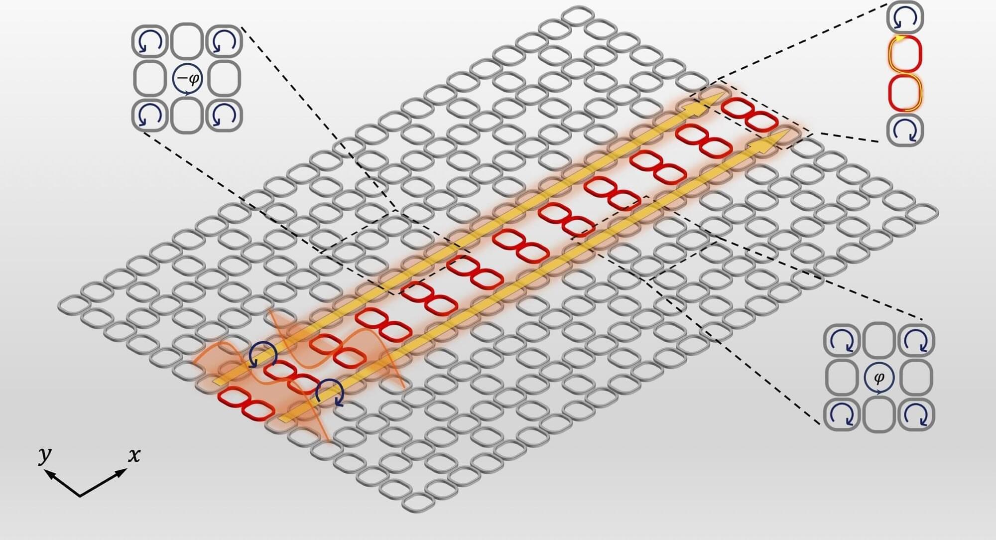
What occurs during the melting process in two-dimensional systems at the microscopic level? Researchers at Johannes Gutenberg University Mainz (JGU) have explored this phenomenon in thin magnetic layers.

“By utilizing skyrmions, i.e., miniature magnetic vortices, we were able to directly observe, for the first time, the transition of a two-dimensional ordered structure into a disordered state at the in real time,” explained Raphael Gruber, who conducted the research within the working group of Professor Mathias Kläui at the JGU Institute of Physics.

The findings, published in Nature Nanotechnology, are fundamental to a deeper understanding of melting processes in two dimensions and the behavior of skyrmions, which may revolutionize future data storage technologies.

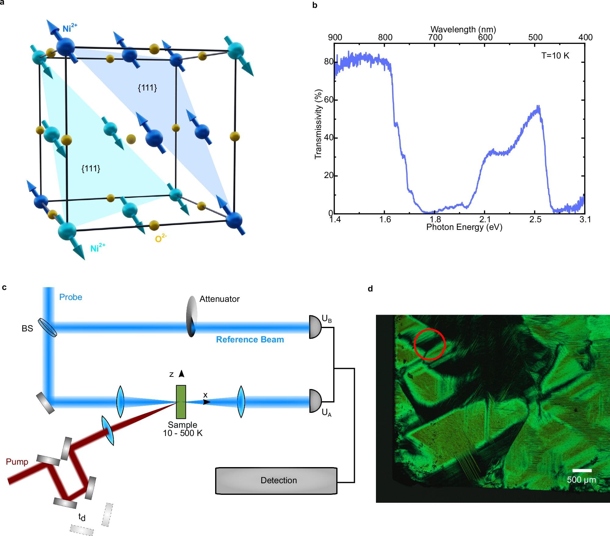
Common crystal proves ideal for low-temperature light technology

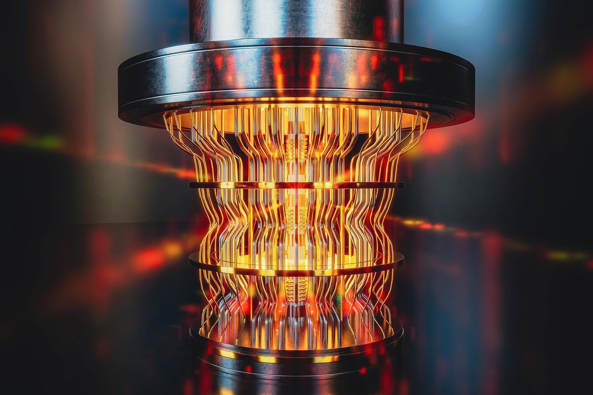
Superconductivity and quantum computing are two fields that have seeped from theoretical circles into popular consciousness. The 2025 Nobel Prize in physics was awarded for work in superconducting quantum circuits that could drive ultra-powerful computers. But what may be less well known is that these promising technologies are often possible only at cryogenic temperatures—near absolute zero. Unfortunately, few materials can handle such extremes. Their cherished physical properties disappear when the chill is on.

In a new paper published in Science, however, a team of engineers at Stanford University spotlights a promising material—strontium titanate, or STO for short—where the optical and mechanical characteristics do not decline at extreme low temperatures, but actually get significantly better, outperforming existing materials by a wide margin.

They believe these findings suggest that STO could become the building block for new light-based and mechanical cryogenic devices that push , , and other fields to the next level.

Microscopic ‘ocean’ on a chip reveals new nonlinear wave behavior

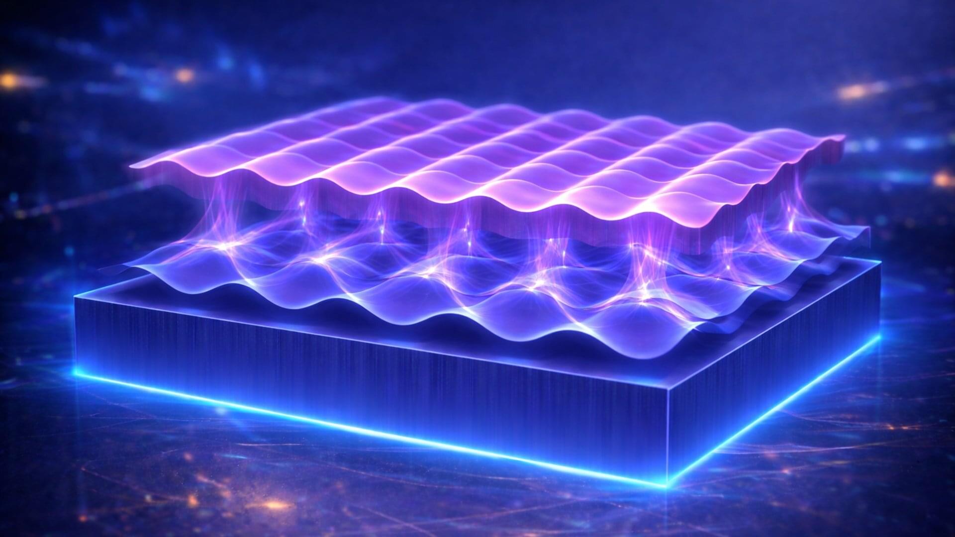
University of Queensland researchers have created a microscopic “ocean” on a silicon chip to miniaturize the study of wave dynamics. The device, made at UQ’s School of Mathematics and Physics, uses a layer of superfluid helium only a few millionths of a millimeter thick on a chip smaller than a grain of rice.

The work is published in the journal Science.

Dr. Christopher Baker said it was the world’s smallest wave tank, with the quantum properties of superfluid helium allowing it to flow without resistance, unlike classical fluids such as water, which become immobilized by viscosity at such small scales.

Novel carbon nanotube-based transistors reach THz frequencies

Carbon nanotubes (CNTs), cylindrical nanostructures made of carbon atoms arranged in a hexagonal lattice, have proved to be promising for the fabrication of various electronic devices. In fact, these structures exhibit outstanding electrical conductivity and mechanical strength, both of which are highly favorable for the development of transistors (i.e., the devices that control the flow of current in electronics).

In recent years, several have started using CNTs to develop various electronics, including metal-oxide-semiconductor field-effect transistors (MOSFETs). MOSFETs are transistors that control the flow of current through a semiconducting channel utilizing an applied to a gate electrode.

Notably, when arrays of CNTs are used to develop MOSFETs, they can operate at (RF), the range of electromagnetic waves that support wireless communication. The resulting MOSFETs could thus be particularly advantageous for the advancement of wireless communication systems and technologies.

Development of revolutionizing photo-induced microscopy and its use around the globe celebrated in new publication

Photo-induced force microscopy began as a concept in the mind of Kumar Wickramasinghe when he was employed by IBM in the early years of the new millennium. After he came to the University of California, Irvine in 2006, the concept evolved into an invention that would revolutionize research by enabling scientists to study the fundamental characteristics of matter at nanoscale resolution.

Since the earliest experimental uses of PiFM around 2010, the device, which reveals the chemical composition and spatial organization of materials at the , has become a tool of choice for researchers in fields as diverse as biology, geology, materials science and even advanced electronics manufacturing.

“This is the story of a technology that was inspired by work at IBM, was invented and developed at UC Irvine, then got spun off, and now we have instruments on all continents across the world except for Antarctica,” says Wickramasinghe, Henry Samueli Endowed Chair and Distinguished Professor emeritus of electrical engineering and computer science who now holds the title of UC Irvine Distinguished Research Professor. “Almost anywhere serious research is happening, there are people out there who are using PiFM to discover new things.”

Shape memory polymers with nanotips help solve micro-LED chip transfer problem

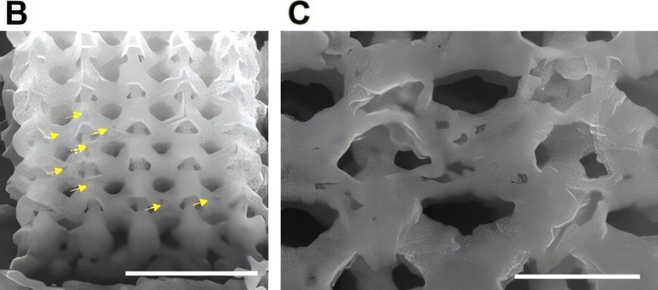
A research team at Pohang University of Science and Technology (POSTECH), has developed a novel dry adhesive technology that allows everything from microscale electronic components to common household materials to be easily attached and detached.

The study was recently published in the journal Nature Communications, and the team was led by Professor Seok Kim in collaboration with Professor Kihun Kim (POSTECH), Professor Namjoong Kim (Gachon University), Professor Haneol Lee (Chonbuk National University), and Dr. Chang-Hee Son (University of Connecticut, U.S.).

Micro-LEDs, a next-generation display technology, offer significant advantages such as higher brightness, longer lifespan, and the ability to enable flexible and transparent displays. However, transferring micro-LED chips—thinner than a strand of hair—onto target substrates with high precision and minimal residue has been a persistent challenge. Conventional methods relying on liquid adhesives or specialized films often result in overly complex processes, poor alignment accuracy, and residual contamination.

Texas company makes $60B semiconductor investment in Texas, Utah

The $60 billion investment involves building or expanding seven chip-making facilities that Texas Instruments has in Sherman, Texas; Richardson, Texas; and Lehi, Utah. Notably, the North Texas city of Sherman will get two new facilities as part of Texas Instruments’ vision to manufacture hundreds of millions of chips daily.

The move comes a few years after the Biden Administration supported companies such as Texas Instruments with funding through the Chips and Science Act. Earlier this month, U.S. Secretary of Commerce Howard Lutnick said the Commerce Department is renegotiating some of its contracts.

And as President Donald Trump has been pushing for more U.S.-based manufacturing, Lutnick celebrated the Wednesday announcement from Texas Instruments.

Saturday Citations: Yet another solution for universal expansion; computing with brain organoids

This week, researchers reported the discovery of four Late Bronze Age stone megastructures likely used for trapping herds of wild animals. Physicists have proven that a central law of thermodynamics does not apply to atomic-scale objects that are linked via quantum correlation. And two Australian Ph.D. students coded a software solution for the James Webb Space Telescope’s Aperture Masking Interferometer, which has been producing blurry images.

Additionally, researchers are networking tiny human brain organoids into a computing substrate; have proposed that environmental lead exposure may have influenced early human brain evolution; and physicists have provided a to explain accelerating universal expansion without :

Algorithm maps genetic connection between Alzheimer’s and specific neurons

The number of people living with dementia worldwide was estimated at 57 million in 2021 with nearly 10 million new cases recorded each year. In the U.S., dementia impacts more than 6 million lives, and the number of new cases is expected to double over the next few decades, according to a 2025 study. Despite advancements in the field, a full understanding of disease-causing mechanisms is still lacking.

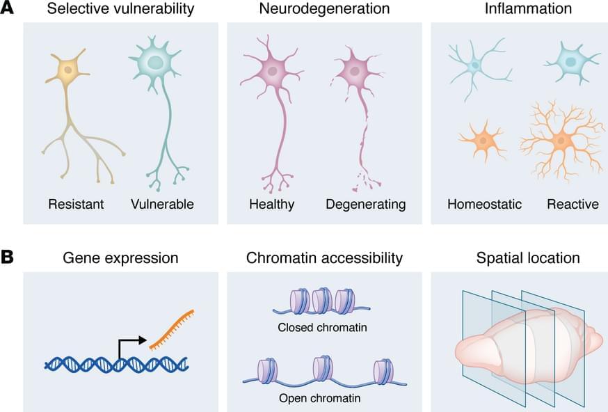
To address this gap, Rice University researchers and collaborators at Boston University have developed a that can help identify which specific types of cells in the body are genetically linked to complex human traits and diseases, including in forms of dementia such as Alzheimer’s and Parkinson’s.

Known as “Single-cell Expression Integration System for Mapping genetically implicated Cell types,” or seismic, the tool helped the team hone in on genetic vulnerabilities in memory-making brain cells that link them to Alzheimer’s ⎯ the first to establish an association based on a genetic link between the disease and these specific neurons. The algorithm outperforms existing tools for identifying that are potentially relevant in complex diseases and is applicable in disease contexts beyond dementia.

Quantum Systems Modeled Without Prior Assumptions

An improved algorithm for learning the static and dynamic properties of a quantum system could have applications in quantum computing, simulation, and sensing.

Quantum systems are notoriously hard to study, control, and simulate. One key reason is that their full characterization requires a vast amount of information. Fortunately, in the past decade, scientists have shown that many physical properties of a quantum system can be efficiently predicted using much less information [1, 2]. Moreover, researchers have built quantum sensors that can measure these properties with a much smaller uncertainty compared with the best classical sensors [3]. Nevertheless, it has been difficult to achieve both efficient predictions and precise measurements at the same time. Now, building on previous breakthroughs in the field, Hong-Ye Hu at Harvard University and his colleagues have demonstrated a new algorithm that characterizes quantum systems of any size with optimal efficiency and precision [4].

/* */