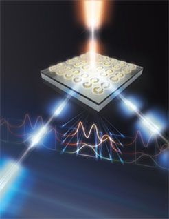
A team built a specialized, layered structure with tiny metallic cavities that improves the light conversion efficiency by orders of magnitude.
Artist’s rendering of an incident laser beam (top of the figure) illuminating an array of nanoscale gold resonators on the surface of a “quantum well” semiconductor (slab in figure). (A quantum well is a thin layer that can restrict the movement of electrons to that layer.) The incoming laser beam interacts with the array and the quantum wells and is converted into two new laser beams with different wavelengths. Changing the size, shape, and arrangement of the resonators can be used for beam focusing, beam steering, or control of the beam’s angular momentum. (Image: Sandia National Laboratories)
The new concept explained in the studies can open doors for advanced lasers for optical communications and efficient manufacturing. It can also support efforts to miniaturize optical components for high-speed computing, telecommunications, cameras, and quantum computing that will solve computational problems currently intractable by today’s supercomputers.
